Can I Combine Inkjet Printing Process And Nanotechnology For 3D Printed Electronics?

Inkjet-based 3D printing uses tiny bits of materials to create cool electronic parts layer by layer. It works like a super smart printer, building things one tiny layer at a time, creating innovative 3d electronics applications.
Can I Combine Inkjet 3d Printing Process and Nano Technology in Electronics?
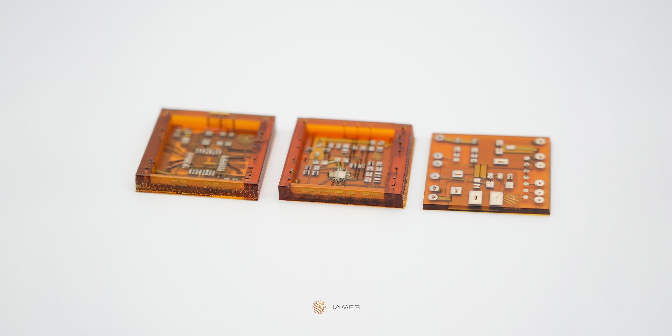
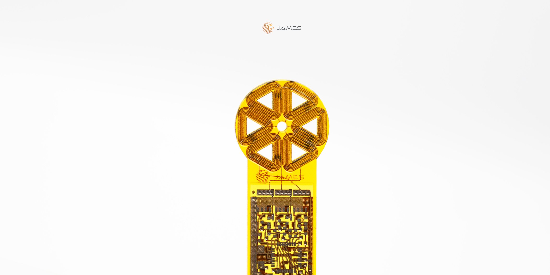
Inkjet-based 3D printing is revolutionizing electronics manufacturing with its low-temperature, low-pressure process. This additive manufacturing technique involves depositing layers of liquid materials or solid suspensions using an inkjet printhead. By precisely layering conductive, semiconductive, and insulating materials, complex electronic components and circuits are created, representing a significant advancement in electrical engineering.
Utilizing nanotechnology, this process manipulates matter at the atomic level, enhancing the design and functionality of electronic devices. J.A.M.E.S is at the forefront of this innovation, integrating inkjet 3D printing into their daily engineering work to push the boundaries of what is possible in electronics manufacturing.
But What About Nano Technology in 3d Printing Electronics?
Nanotechnology spans physics, chemistry, biology, engineering, and materials science, focusing on creating and manipulating nanomaterials with unique properties. In electronics manufacturing, we use nanoparticles, like silver ink, in 3D printing. This process lets us deposit polymers, dielectric nanoparticles, and conductive nanoparticles, making it versatile and adaptable to various materials.
Related Articles


J.A.M.E.S. At The 32nd FED Conference - Showcasing Innovation In 3D-Printed Electronics


Catalyzing Transformation In High-Tech Domains: Consumer Electronics And The Automotive Sector Through XTPL S.A.’s Innovations
