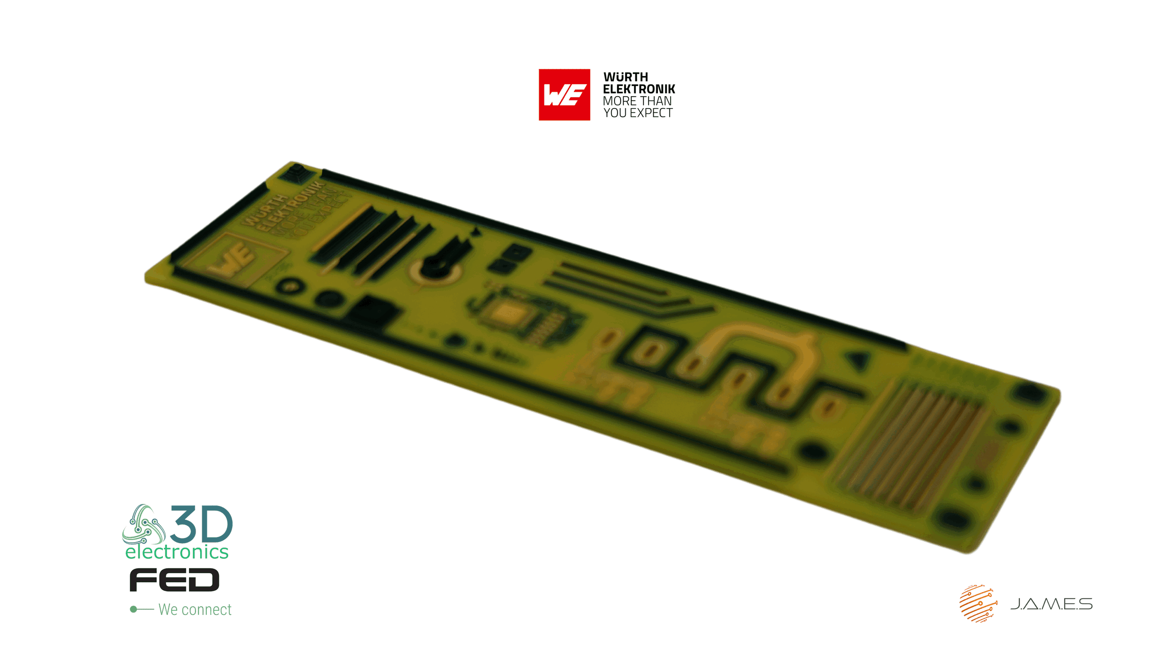
FED - 3D Printed Digital Solder Mask

“Design rules for digital solder mask- what are the current possibilities?”
At the 32. FED conference 2024 in Ulm
presentation by Michael Matthes,
Specialist Design/Layout and Measurement
at Würth Elektronik
Würth Elektronik Demonstrates the
new possibilities of additively applied solder mask, also known as s.mask.
An outstanding innovation is 3D printing in height.
Similar to conventional 3D printing with materials such as PLA or ABS, the solder mask is applied in layers with a thickness of a few μm per layer.
In a certain area, vertical edges of the paint can be realized, but only up to a certain height.
In addition, a certain gradation of the flanks is necessary.
In this way, structure heights of up to 1400 μm (1.4 mm) can be achieved.
Comments
Michael Schleicher
1mo ago
From my perspective approach of the digitals soldermask is one of the future "hidden champions" related to 3D printing or "hybrid 3D printing" within electronic design and electronic manufacturing. It's like a "eye opener" or the first step to improve understanding of 3D printing in electronic applicaions.Even if it seems rather unspectacular or even unsexy at first glance. Good work Michael!
Andreas Salomon
1mo ago
Hallo Michael, thank you for publishing! I know you are in contact with different tool providers for this activities - hope you'll keep us updated about that as well as for the FED whitepaper Articles for "AME Classification" Cheers Andi Salomon
Related Articles

Voltera
1 Like
1 Like
Voltera: Print Multilayer Flexible And Stretchable Circuits With NOVA
04.02.2025

J.A.M.E.S GmbH
0 Likes
0 Likes
Researching Additively Manufactured Electronics To Improve The Quality Of Life
25.07.2024

Fachverband Elektronikdesign und -fertigung e. V.
4 Likes
4 Likes
FED White Paper Edition 2024 - Part 5 - Design Tools For 3D Electronics
06.09.2024
Featured Partners
About Us
© 2025 J.A.M.E.S GmbH.


