FED White Paper Edition 2024 - PART 3 - AME Class 3 And Class 4
Part 3
AME Class 3 and Class 4 of the new edition White Paper
Classification of additive manufacturing and 3D-printing processes for electronics
Table of Contents
Class 3 – Printed Multidimensional Substrate
“Class 3" defines the application, where both, the mechanical substrate and the electronics, are manufactured. This means, that the product manufactured using this technology can take on a freely designable three-dimensional shape and, as a “fully additive” process, the electronics can be applied to the inside as well as the outside surfaces of the substrate. As described in “Class 1” and “Class 2”, the additive layers can be applied using a wide variety of processes and technologies. Multilayer conductor layers can also be separated by partially applied insulating layers that may also be the substrate material.
By using suitable materials such as resistor paste or ferromagnetic paste, components such as resistors, capacitors, inductors or “light guide structures” can be applied directly using printing processes. Very complex systems can be realized in the smallest of spaces using the appropriate production technologies. The variety of shapes of the printed body seems endless.
Application and Drying (curing/hardening) of the Material
The material is applied layer by layer in the exact position, depending on the process used. Depending on the material composition curing takes place using various sources such as UV, IR, microwaves or dryers. The material properties (conductivity, insulation strength) are adjusted by the inks and pastes and are achieved after curing. This allows to print semi-conductive layers, light guides or resistors. Printed material can, for example, take on the function of solder resist or conformal coating.
Examples of Material Application and Drying (curing/hardening)
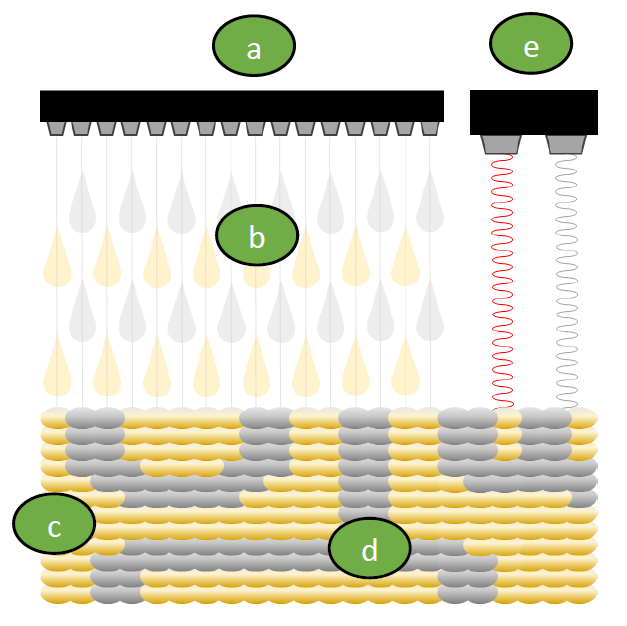
Micro dispensing is a possible method for Additively Manufactured “Class 3” electronics:
a) Micro-dispensing nozzles: application of fluids according to the DPI of the nozzles (DoD).
The print volume and DPI correlate. Multi-material printers eject the different materials from different nozzles. Several print heads can be operated in parallel in parallel to increase throughput and reduce process-time.
b) The ejected fluid droplets in picolitres (pl)
c) Non-conductive material
(cured: amber/yellow)
d) Conductive material (cured, gray)
e) Energy sources for hardening the material. Using different wavelengths and optimal matched to the to the applied material:
UV, IR or microwave. After hardening, the sub-strate must be cured e.g.: using thermal ovens.
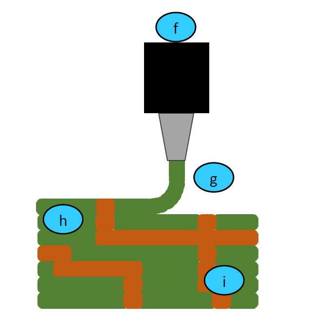
Extrusion and dispensing are possible methods for Additively Manufactured “Class 3” Electronics:
f) Extrusion or dispensing of pasty materials, usually with chemical or thermal curing.
Multi-material application is possible.
g) The distance from nozzle to substrate is rather small.
h) Hardened (cured) dielectric material (green).
i) Hardened (cured) conductive material (brown).
Micro dispensing (above) and extrusion (below) of the base material are two methods of printing spatial circuit carriers (3D shape)
Internal and External Shape (contour)
The materials can be printed laterally, vertically or in different directions (angles) using these processes. If needed, it’s possible to print only planar structures. However, one advantage is that 3-dimensional shapes can be created.
The substrate can be printed on three-dimensional or bionic shapes (free-form approach) by utilizing systems with 4-6 axes. Shapes already in use today include cones, pyramids or grid structures for transmitting and receiving antennas or RF filters. The printing principle allows it, to create shapes that can be used without further mechanical processing (no drilling, milling or cutting, …). It is possible to create openings, channels (for fluids) or complex internal structures.
It is possible to create rigid, flexible, rigid-flexible or even stretchable substrates within one printing process. Another option is, to add specific structures for reinforcement or other functions.
Advantages and Benefits
The possibilities offered by the different printing process result in a wide range of combinations of printed materials. The "free-form approach” also allows an almost infinite variety of shapes for the mechanical and electrical structures in the final products.
Other exemplary advantages of "Class 3" printed components and functions are:
- Three-dimensional (3D) outline of the substrate
- Application of very thick and very thin structures: rigid, flexible, reinforced, 3D and 4D
- Printing of passive HF-structures: antennas, filters, etc.
- Structural optimization through organic or bionic (generative) forms
- Electrical contacting of components terminals e.g.: solderless connection
- Solder resist: additively applied layers or improved high voltage insulation
- Depending on the process, large components can also be realized, e.g.: automotive parts, drones or aircraft wings.
Class 4 - 3D Printed Substrate + Printed Components
The “Class 4" defines the application of one or more conductive, semi-conductive or non-conductive functional layers without a carrier, as already described in "Class 3". The addition to the previous classes is, that active or passive components are placed within the printing processes and connected using printing technologies. These components are characterized by the fact, that it is possible to embedded them within the in the 3D product and/or added to the outer surfaces of the 3D body. This should enable a further increase in the integration density and functionality of the 3D product or a cost saving.
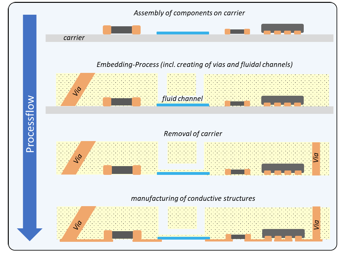
In the process a 3-dimensional component substrate is created using the one of the specified AME printing technologies. Due to "printed cavities" it is possible to assemble electrical or electromechanical component. Alternatively the components can also be assembled in an intermediate step and then "overprinted". In a further step conductive layers are applied in such a way to achieve an electrical contact with the component terminals. This eliminates the need for a soldering or bonding process, for example, which can minimize materials degradation processes, cable lengths or contact resistances.
Nevertheless as in "Class 3" some components such as resistors, capacitors, inductors or light guide structures can be applied directly in printing processes with the use of suitable materials (e.g. resistor paste, optically conductive materials). By carrying out the process steps listed above several times highly complex systems can be realized in the smallest volume.
An example for the process steps of an Additively Manufactured functional carrier (substrate)
with embedded components and fluid channels of Class 4
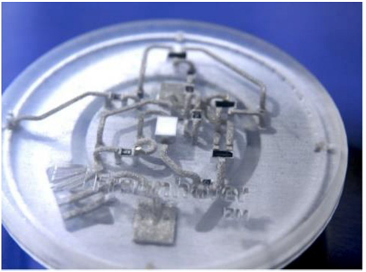
Example for “Class 4”: Transparent substrate with embedded electronics (Source: Fraunhofer IZM)
Go Back to AME Classification Overview
the FED working group for 3D electronics is
Introducing the 5 Classes/Types of process 3D printed electronics
Related Articles


