FED White Paper Edition 2024 - Part 5 - Design Tools For 3D Electronics

Part 5,
Design tools for 3D electronics
out of the new edition White Paper
"Classification of additive manufacturing and 3D-printing processes for electronics"
Design Tools for 3D Electronics
A crucial criterion for the design of electronic 3D systems is the question which toolchain can be used to achieve the goal. The short answer is: there is currently no 100 % suitable tool or toolchain available. Within “classic design tool-chain”, the so-called mCAD tools (mechanical CAD tool) lack the information on electrical component information and connections as well as the resulting electrical netlist.
“Classic eCAD tool-chain” (electrical CAD tools) are designed in such a way, that the systems work layer-related and the information on layer thicknesses and function is described in extra guided settings (tables and spreadsheets). In the meantime a 3D representation can be "triggered" via an extra function.
Routing options, e.g.: 3D contour with contour-following conductor routing
The tools have been refined over the years and provided with semi-automatic functions, that will be supported via “Artificial-Technologies (AI) in the near future. Within PCB design, the "online DRC", "push and shove", "plow" and other modes, support the designer. Transferring such functions to the 3D construction space could become a challenge. Example for this are vertical connections, so-called "vias", which connect tracks from layer to layer. As there are no "layers" in the 3D construction, this specific function is no longer required. Vertical connections can be routed at any angle and to any depth as well as around outer surfaces. This raises the question of how 3D online DRC or the semi-automatic functions mentioned above can be pictured (screen) and implemented here.
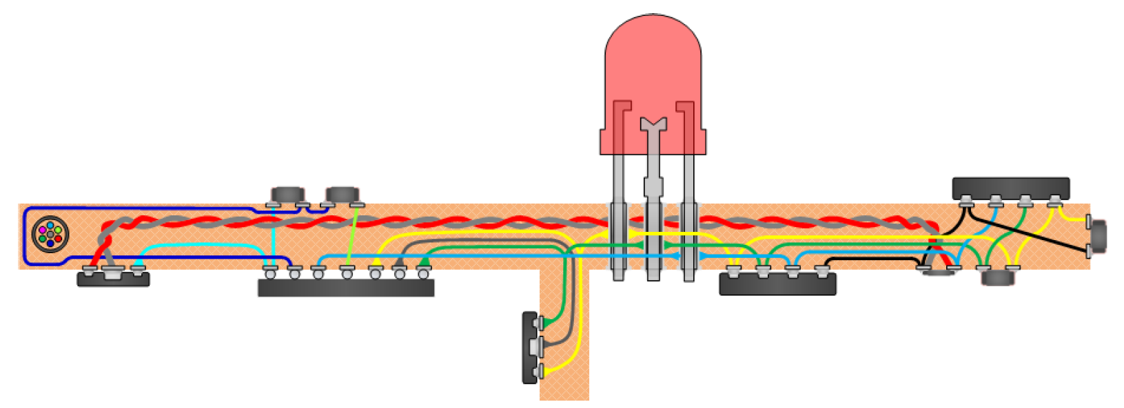
Routing options, e.g.: 3D contour, twisted pair
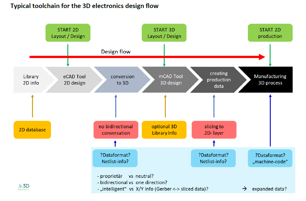
The first promising approaches to importing three-dimensional bodies created with the help of mCAD tools into eCAD tools have been developed over the years. The eCAD tool offers the option of placing the components on the outer layers and implementing the routing. Tool providers have been trying few years ago to enable simple data exchange with the help of neutral or proprietary data formats. Only very few of the solutions currently on offer are "barrier-free” or seamless.
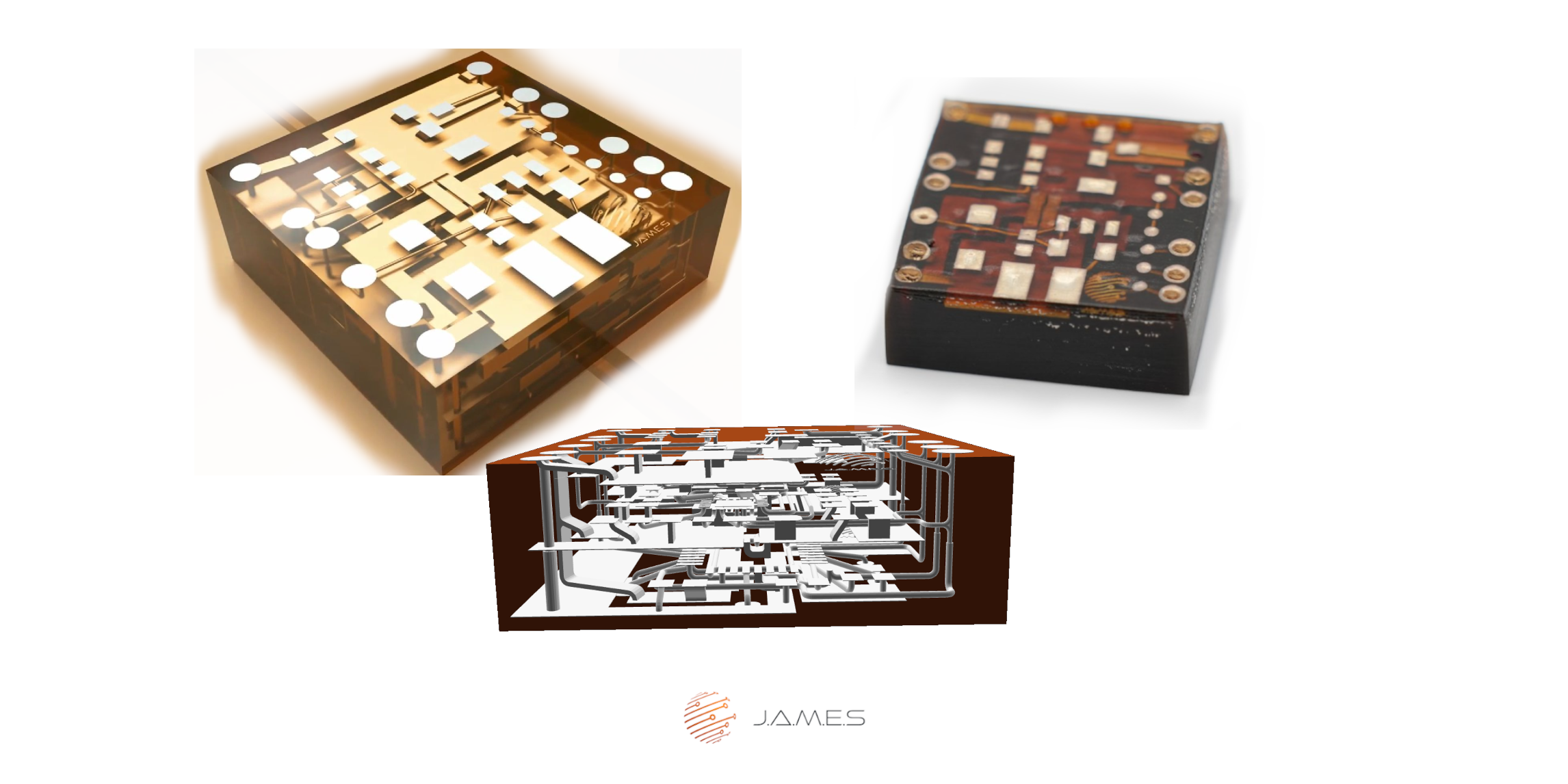
RF-Synthesizer with full 3D-wiring module, with integrated components and shielded cables
see J.A.M.E.S Article RF Synthesizer - 3D Heterogeneous Integration
Which functions might be needed in the future? 3D printing is often associated with optimized material usage. Material is printed, where it is needed and nothing is printed, where no material is required. Appropriate tools should make it possible to design bionic or generic shapes.
As a result the 3D body must be developed and designed together with the conductor structures. In order to achieve this goal a mechanical-structural simulation is required in parallel to the electronic simulation, for example.
First tool providers have identified some of these gaps and are trying to simplify data migration with corresponding software platforms outside of the actual eCAD and mCAD tool-chain. Most of the 2023 developed projects will be developed with the help of one’s own initiative, workarounds, drawings and a huge amount of direct communication. The majority of 3D printers achieve their shape with a job of a specific material type. Multi-material printing of conductive and non-conductive materials within one printing process has so far been a marginal phenomenon.
However, this is the prerequisite for printing a circuit carrier (substrate). Within mCAD design the focus is on the shape, which the function is derived. In eCAD design, it is generally the other way round: the function leads to a form.
Considerable effort is still required to make 3D electronics a success. One aim of the classification is to indicate the complexity of the respective class and to derive which tools or toolchain are necessary for the implementation of the respective project.
Requirements for the Data Formats
A closer look at the various used toolchains, both for mCAD and eCAD, reveals that a wide variety of manufacturing data formats have developed over the years. Of course this also reflects the technical development over this time.
A universal data format for the description of the mechanical form, the electronic information and the components used, is not yet available. The question currently remains, as to whether it is possible to extend an eCAD data set with corresponding "mechanical" functionality or vice versa? Here it is necessary for both tool worlds to move towards each other in order to develop the best possible data format. This is where the biggest gap currently exist!
A closer look at this FED-classification shows, that previous eCAD data formats are still suitable for "Class 1" applications. "Class 2" systems must be analyzed in detail and it must be considered which data format can be used sensibly. From "Class 3" onwards, the previously known eCAD formats are no longer sufficient. With increasing complexity it is also necessary to define appropriate tests (electrical, mechanical, optical) of the functions created and to determine an interim result "in-situ" or to verify the status.
With the help of the classification described, it is possible to carry out a gap analysis in order to develop or further develop corresponding data formats.
Compared to traditional electronics with established design workflows, the construction and design of "Additively Manufactured 3D Electronics" requires far more preliminary planning and consideration of the sometimes sequential production processes.
The layered structure enables the integration of SMD and printed components, but requires early planning of the production steps and processes. Developers must carry out preliminary evaluations of different processes and technology variants. Otherwise it may turn out during production that manufacturing is not feasible at all.
Production and Scalability
Regardless of the printing process the complexity of the project to be printed shape the basis of the evaluation for production and the resulting scalability. The different possibilities of the individual processes must be matched to the product or system.
The abundance of existing (and future) processes often obscures, which processes can be used to achieve a high print throughput or a high number of printed parts in a short time. This goes hand in hand with the question of how to scale up from prototype printing to series production. The various processes play a decisive role here.
The following questions can help with the evaluation and decision-making process:
- The speed of the printing process: laser vs. dispensing
- Parallelization of printheads and dispensing systems
- The x/y size of the available working area
- The z-travel of the print head or alternatively the area of operations
- Material consumption through "resin basin" or powder bed
- Cleaning and post-treatment of residues from the printing process
- Need for supporting structures and the associated reworking
- Monitoring and verification of the pressure by e.g. in-situ measuring and testing procedures
Go Back to AME Classification Overview
the FED working group for 3D electronics is
Introducing the 5 Classes/Types of process 3D printed electronics
Related Articles


