FED: Klettwelding AVT Process
Nov 27, 2024
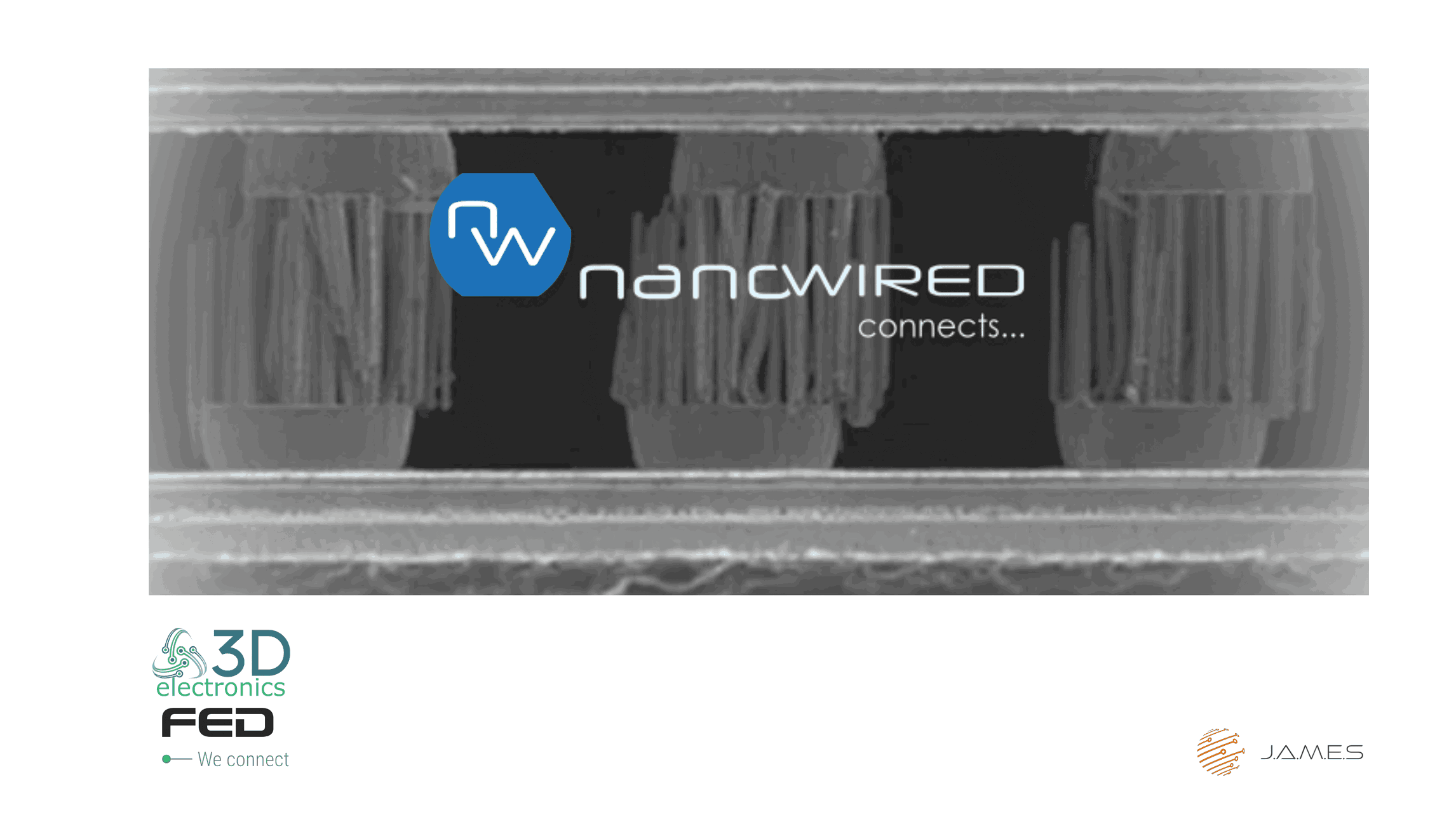
Klettwelding AVT process - a reliable replacement of soldered or bonded connections
At the 32. FED conference 2024 in Ulm
presentation by Dr. Sebastian Quednau,
NanoWired Presentation
Dr. Sebastian Quednau gives an overview about
-
NanoWired company
-
NanoWiring process with large variety of substrates
-
Joining procedures (Klettwelding / Klettsintering / Klettglueing)
-
NanoWired technology and different morphologies
-
Project examples with NanoWired - NANO-AVT
-
connecting PCB's
-
DC/DC-converter for 20 kW
-
robust RF-connection for signals > 20 GHz
-
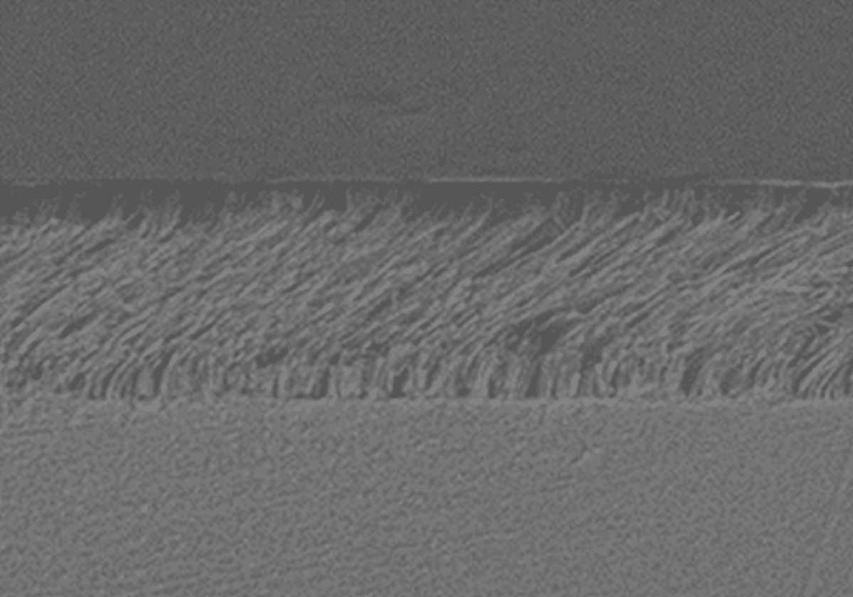
NanoWired Klettwelding
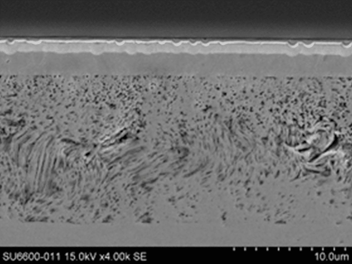
NanoWired Klettsintering
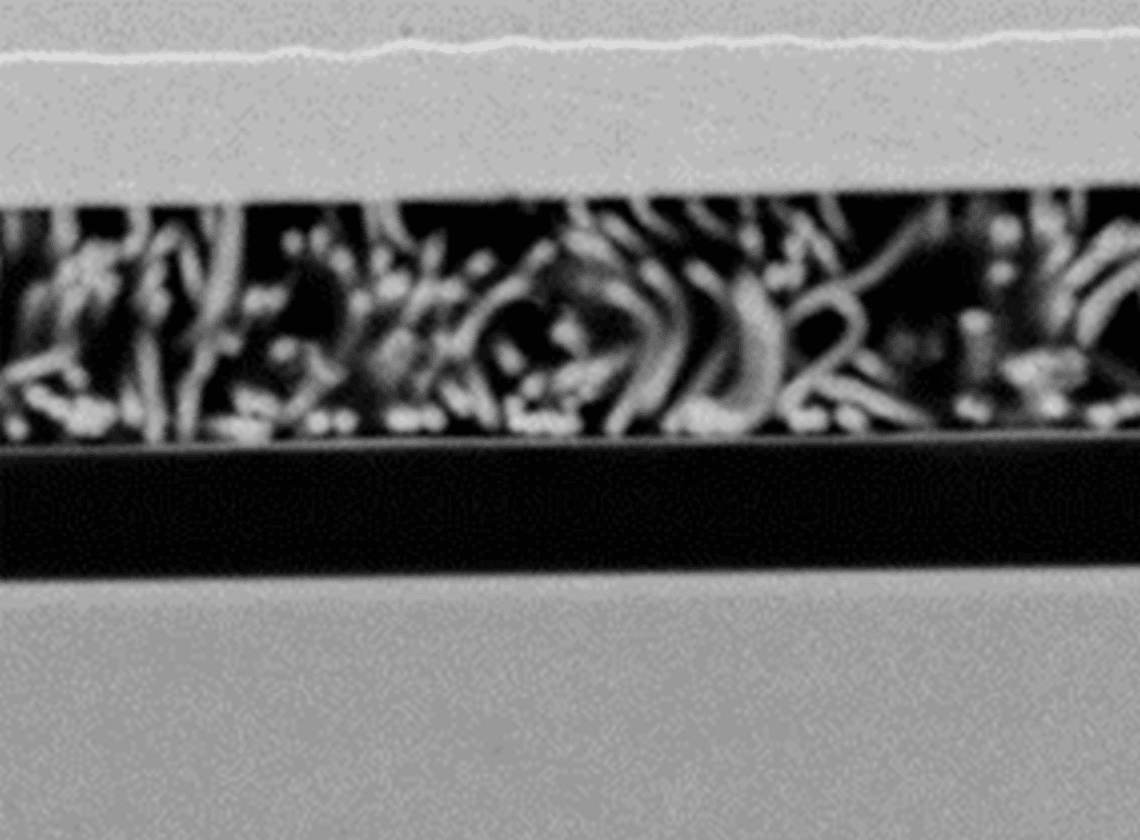
NanoWired Klettglueing
Related Articles

Fachverband Elektronikdesign und -fertigung e. V.
3 Likes
3 Likes
32. FED-Conference 18./19. September Ulm
20.06.2024

Fachverband Elektronikdesign und -fertigung e. V.
3 Likes
3 Likes
Pan-European Electronics Design Conference - Abstract Submission
10.06.2024

Fachverband Elektronikdesign und -fertigung e. V.
4 Likes
4 Likes
FED - 3D-Multilayer Devices (3D-MLD)
13.02.2025

J.A.M.E.S GmbH
8 Likes
8 Likes
Reflecting On Electronica 2024: Experiences, Insights, And New Opportunities
02.12.2024


Featured Partners
About Us
© 2025 J.A.M.E.S GmbH.