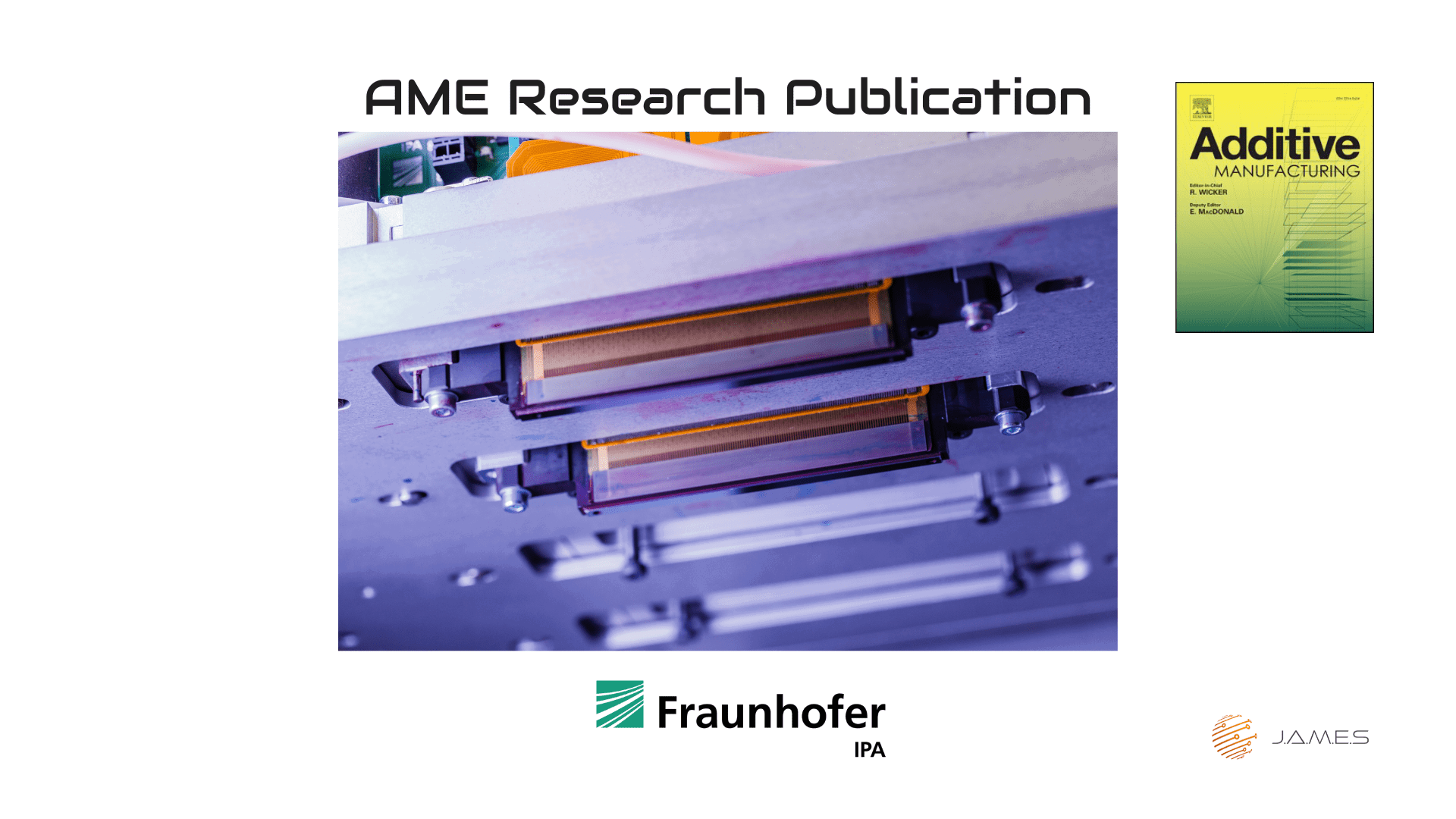
FhG IPA - Material Jetting For Advanced Applications: A State-of-the-art Review, Gaps And Future Directions
on
Science Direct
Additive Manufacturing
Volume 60, Part A, December 2022, 103270
by
Ahmed Elkaseer, Karin J. Chen, Veit Hagenmeyer, Steffen G. Scholz from KIT Karlsruhe Institute of Technology, Germany
Jan C. Janhsen, Oliver Refle, from Fraunhofer IPA, Germany
and Faculty of Engineering, Port Said University, Port Fouad, Egypt
ABSTRACT
The proven ability of additive manufacturing (AM, also known as 3D printing) to fabricate complex components with substantial reductions in material wastage and reduced lead times has made it a key enabling technology for numerous important industrial applications. Of current AM processes, material jetting (MJ) is demonstrating considerable potential for producing multi-material, intricate, 3D components and systems with integrated functionality, with the additional benefit that the process can be easily integrated with other manufacturing procedures.
However, material jetting of functional materials to produce advanced applications still poses numerous technological challenges which hinder its full industrial exploitation. These extend from the limited range of high-performance materials with consistent properties usable for MJ, through the need to enhance the process itself by optimizing the droplet formation process, tuning waveforms for specific processes, modification of substrate and substrate/jetted material interactions, the complexities of curing and post-processing procedures, and the challenge of characterizing the 3D printed parts. In this context, this article attempts to provide a comprehensive discussion of the principles and characteristics of the most recent material jetting technology and reviews the state-of-the-art research and development being conducted.
This review identifies existing gaps with regards to high-performance UV-curable inks, printing behavior of non-Newtonian fluids, optimum jetting and curing strategies and effective measures for achieving high-precision MJ. Future work should bridge the aforementioned gaps in order to improve the performance of the technology, thereby making it more attractive for large-scale adoption by industry and increasing market acceptance and penetration of material jetting for advanced applications.
TOPICS
- Introduction
- Jettable inks
- Characterization of jettable inks
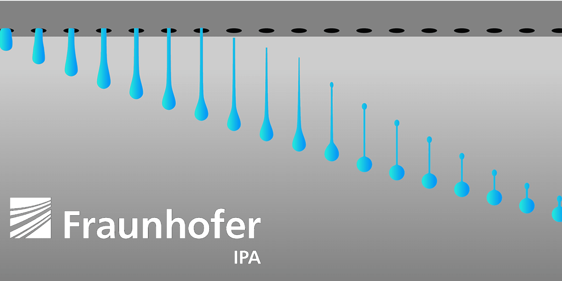
- Drops generation
- Droplet/substrate interaction
- Curing process
- Photopolymerization
- Curing depth
- Curing process
- UV-sources
- Curing strategies
- Quality issues in material jetting
- Shrinkage
- Layer height consistency
- Oxygen inhibition
- Gas dissolvement
- Coffee-ring effect
- Current and potential applications
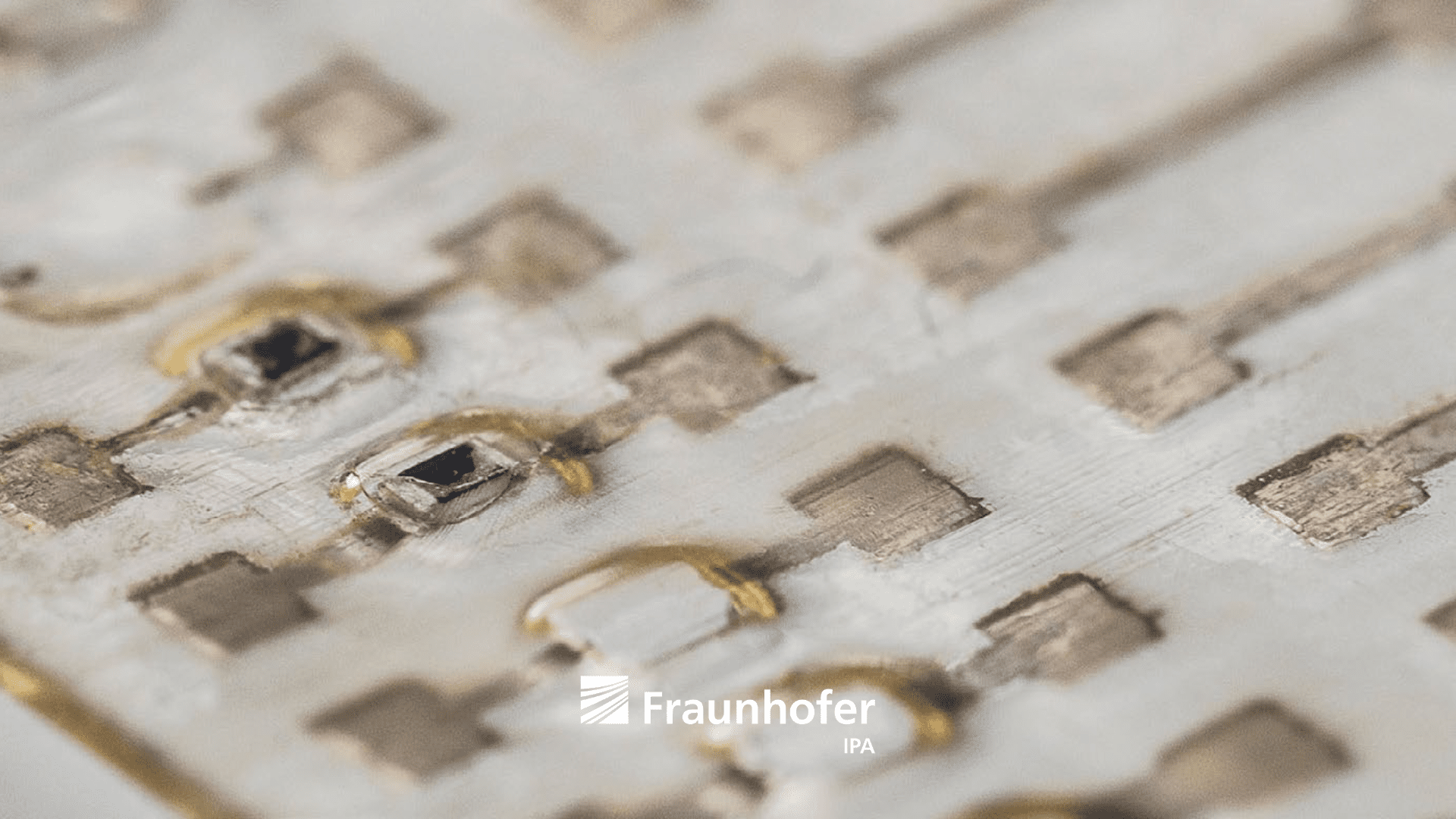
- Printed electronics
- Pressure sensors
- Transistors
- Photoacoustic generators
- Capacitor
- Solar cells
- Quantum dot light-emitting diodes (QLEDs)
- Antennas
- Heating elements
- Thermal insulation thin film
- Smart textile
- Functional membrane
- Anticounterfeit
- Microstructure surface
- 4D-structure
- Chemical, biological and pharmaceutical applications
- Chemical catalyst
- Biological constructs and peptide printing
- Paper chip-based detector
- Material jetting for 3D and 4D applications
- Printed electronics
- Gaps and future prospects
- UV-curable incs in MJ
- Drops generation and layer forma...
- 3D/4D multi-material printing
- Conclusions

Watch and Download the Full Research Publication on
Science Direct
Additive Manufacturing
Related Articles


Doctoral Thesis - Numerical Simulation Of An Additive Manufacturing Process For Low-Impedance Electronics

FED: Additive Processes Improve PCB-quality

