Fraunhofer IKTS

Rough condition? Tough ceramics!
For more than 30 years, Fraunhofer IKTS has been demonstrating the potential of ceramic materials. We develop electronic components that are suitable for use in harsh environments with high thermal, chemical and/or mechanical loads.
Latest Articles


Competence in Additive Ceramics
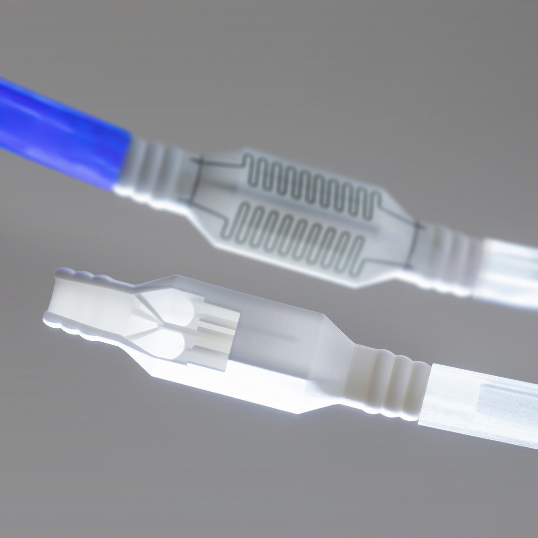
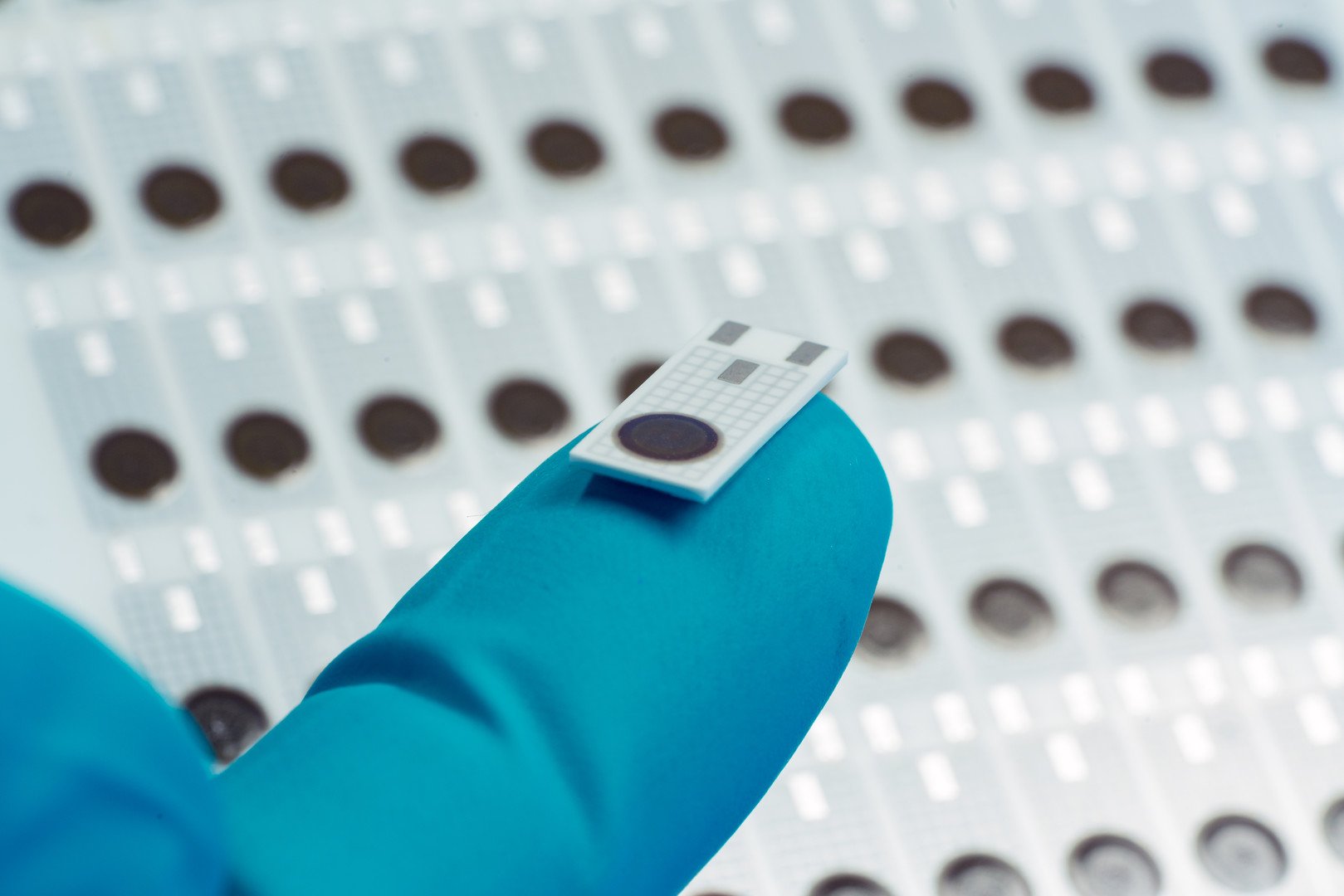
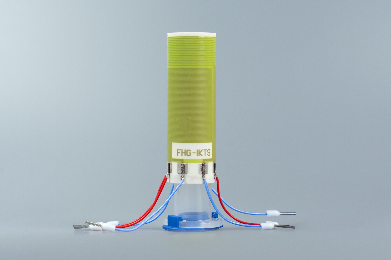
For more than 30 years, Fraunhofer IKTS has been demonstrating the potential of ceramic materials. We develop electronic components that are suitable for use in harsh environments with high thermal, chemical and/or mechanical loads. Additive processes are used for complex geometric requirements. Thick-film and direct-writing technologies can be used to functionalize the components. For this purpose, layers of sensory or actuator active, electrically conductive, thermally conductive and/or insulating pastes or inks are applied and sintered.
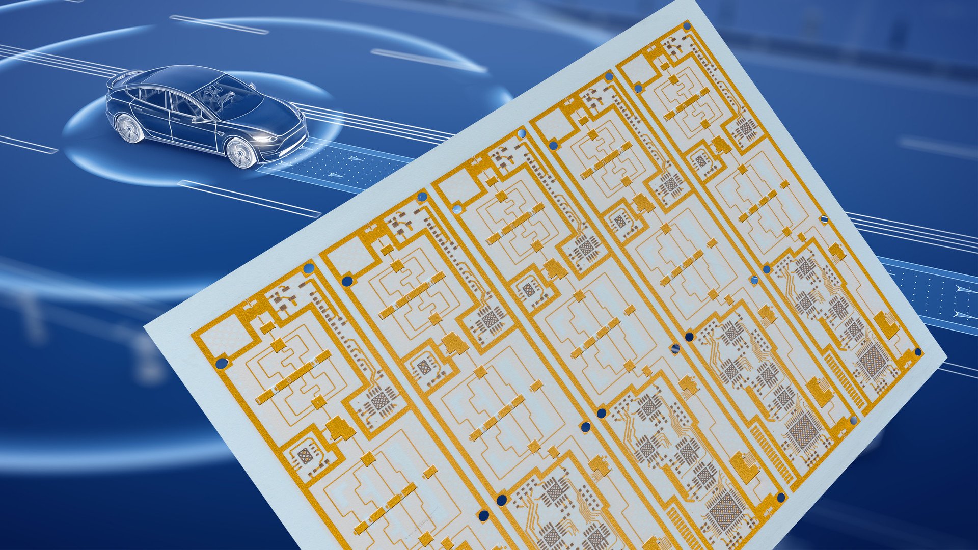
Ceramics as High-Frequency Circuits
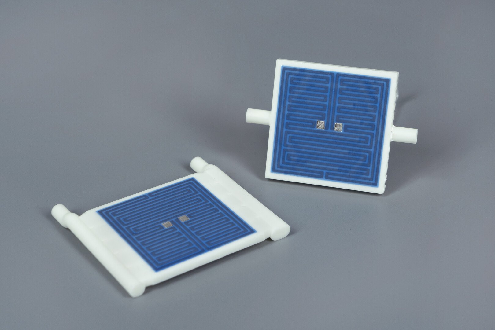
For the manufacture of high-frequency assemblies, all-ceramic or glass-ceramic LTCC materials with their outstanding high-frequency characteristics provide the springboard to the next generation of circuit carriers. LTCC ceramics can be functionalized comparable to printed circuit boards with electrical conducting tracks and provided with internal functional layers or buried structures.
Services Offered
We cover the entire value chain: from material synthesis and powder processing to the development of functional ceramic semi-finished products, component and system design, and process development, right through to functional testing and reliability studies. In the area of AME, the development of customer-specific functional inks/pastes, as well as technology development for 3D metallization and integration, form the main focus of work. For our customers, we can map various scales, ranging from feasibility studies to the development of small series for demonstration purposes to the transfer to mass production.
Technology
The combination of ceramic additive manufacturing and thick-film as well as direct-writing technologies opens up a wide range of new applications for harsh environments
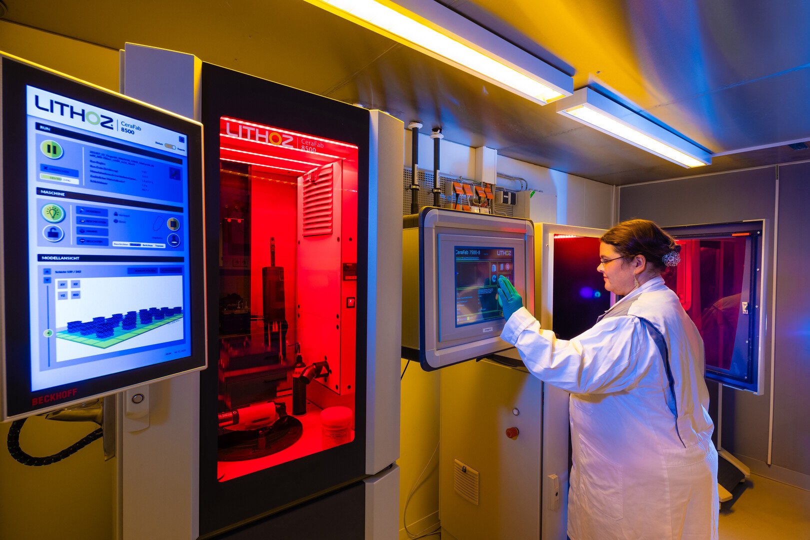
Additive Manufacturing
Additive manufacturing has high innovation potential for ceramic products in terms of design and the ability to produce novel composite and gradient materials.
Functionalization
While additive processes offer new possibilities through their principle, the combination with established thick-film and direct-writing technologies further expands the spectrum of functions, components and applications.
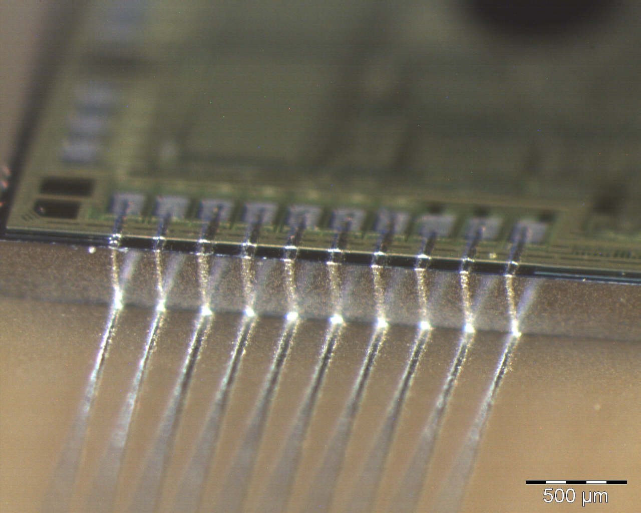
Electronic Packaging
A wide range of packaging technologies such as soldering, bonding, welding, wire bonding or sintered assembly are available for electrical contacting and the assembly of other electronic components.
Applications
The technology combinations presented pave the way for manufacturing applications in electronics and power electronics as well as sensor and energy technology.
Points of Contact