Introducing QuickSiP, A True Technology Game-Changer!

In today’s fast-paced, competitive electronics industry, the drive for miniaturization and innovative design faces significant challenges. As the annual rate of component miniaturization declines, there is a growing need to reduce the size and weight of the electronic systems housing these components. This is where "System in Package" (SiP) technology comes into play.
Understanding SiP and Its Challenges
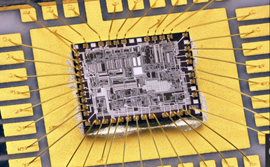
SiP involves bundling multiple integrated circuits on a carrier using various interconnect methods, functioning like a miniature printed circuit board (PCB). SiPs perform most, if not all, functions of an electronic system and are integral to a wide range of devices, from advanced defense systems to intricate medical devices and mobile phones.
However, SiP manufacturers prioritize high-volume production to maximize efficiency and profitability, often sidelining small and medium enterprises or imposing premium costs for their fabrication services. This, combined with other supply chain challenges, makes research and development (R&D) a lengthy and arduous process, stifling innovation, especially for companies focused on high-variety, low-volume manufacturing.
The traditional SiP process involves complex, multistep planning, system design, and die implementation, each fraught with potential delays. Consequently, the R&D cycle can be long and unpredictable, often requiring several iterations to produce a single prototype.
The Birth of QuickSiP
Nano Dimension has embarked on a mission to revolutionize SiP design and manufacturing through Additively Manufactured Electronics (AME), leading to the development of QuickSiP. Initial beta testing has yielded promising and exciting results.
Nano Dimension, a pioneer in AME, introduced the DragonFly IV® system, which uses digital files and 3D simultaneous printing of dielectric and conductive materials to create high-performance, multilayered electronic parts.
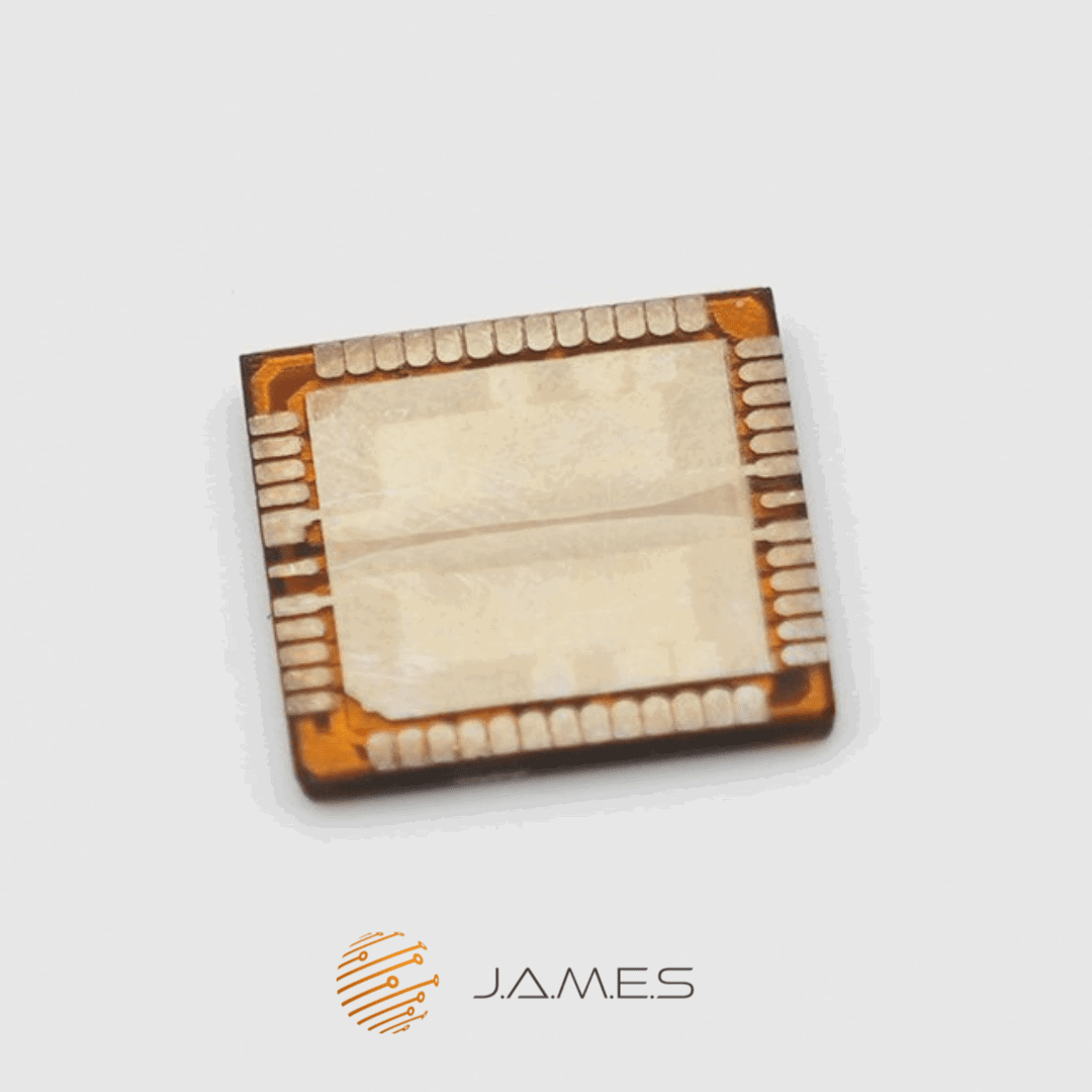
Collaborating with an external partner, Nano Dimension’s technical team is showcasing how SiP structures can be produced using AME technology. This includes generating detailed connectors and precise cavities for mounting components, eliminating the need for drilling. Unlike traditional methods, QuickSiP avoids wire-bonding, instead connecting the bare die to the AME carrier structure using appropriate AME printing processes.
QuickSiP Advantages
QuickSiP promises to drastically reduce prototype development time, facilitating rapid iteration of new electronic products. Academic labs could benefit from immediate one-off designs for experimental purposes, while commercial manufacturers could enjoy shorter development timelines, gaining a competitive edge. The SiP production market is projected to grow at an 8% compound annual growth rate until 2030.
Nano Dimension projects that QuickSiP can slash R&D time from 12 months to just 2 months while achieving significant weight and size reductions and enabling the creation of a variety of low-volume SiPs. The potential for multilayered SiP structures could lead to even more complex and functional designs.
QuickSiP Using DragonFly IV®
After extensive testing, the QuickSiP package dimensions are finalized at 13.2×13.2×1.5mm, with a minimum pad size on the die of 70µm. The package includes components such as 1 MMIC 4W X-band die (QPA1022D), 6 resistors, 3 capacitors, and 2 MOSFET dies.
The team addressed challenges related to registration, creating flat surfaces on printed circuit structures, process automation, material adhesion, and rapid testing of samples. The assembly process is split into three parts:
- Printing the bottom with cavities – approx. 8 hours
- Placing bare dies – approx. 1 hour
- Printing the top with circuitry – approx. 12 hours
There is also potential to automate further and integrate a flip-chip assembly process with a pick-and-place machine.
J.A.M.E.S Conclusion
The success of the DragonFly IV®-generated QuickSiP demonstrates significant potential for transforming the electronics industry. The Nano Dimension team is enthusiastic about the future evolution of this technology and its positive impact across a broad spectrum of products and industries.
If you are interested in more information contact J.A.M.E.S engineering.


