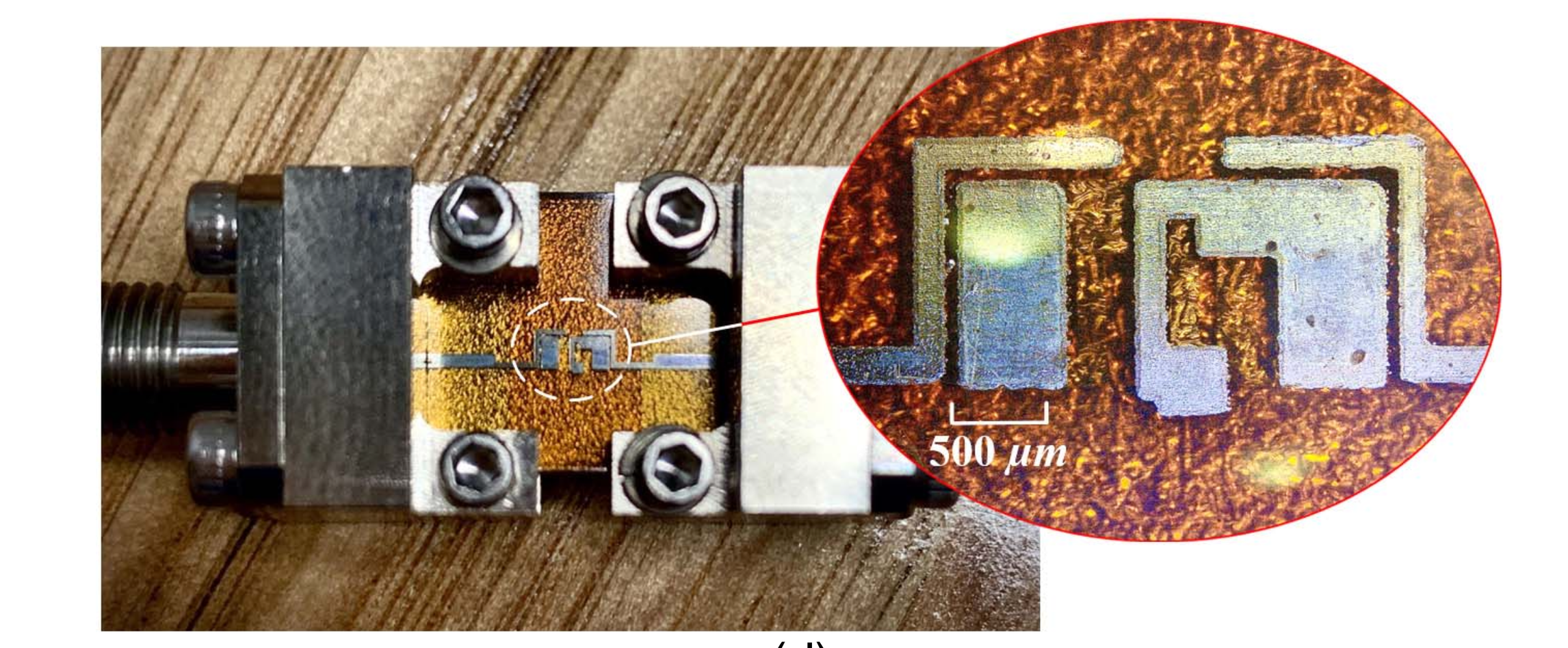
Compact Multilayer Bandpass Filter Using Low-Temperature Additively Manufacturing Solution

This research paper, titled "Compact Multilayer Bandpass Filter Using Low-Temperature Additively Manufacturing Solution," was authored by Mengze Li, Yang Yang, Francesca Iacopi, Minoru Yamada, and Jaim Nulman.
Overview of the Research Paper
This research presents a compact multilayer bandpass filter (BPF) using low-temperature additive manufacturing method. The BPF is realized with multilayered metals and utilizes an AME solution to extrude conductive material and at the same time form a dielectric. The filter designed for use in television broadcasting, radar detection, and satellite communication operates at 12.25 GHz with a bandwidth of 40.8%.
Key highlights include the use of a low-temperature (140°C) process that facilitates the integration of multiple metal layers within a single substrate, enabling device miniaturization. The research employs advanced inkjet printing technology to fabricate 3D components with precise control over the interlayer distance, achieving consistent inductance and capacitance in smaller dimensions. The paper provides a comprehensive analysis of the BPF's equivalent circuit, supported by both mathematical modeling and electromagnetic simulations, showing good agreement with measured results.
Table of Contents
Introduction
- Overview of additive manufacturing technologies and their application in electronic device integration and 3D packaging.
Additively Manufactured Components for BPF Miniaturization
- Details on the use of AME technology to create miniaturized inductors and capacitors.
Multilayer BPF and Its Equivalent Circuit
- Configuration and analysis of the proposed BPF, including its equivalent circuit and mathematical modeling.
Measurement Result
- Comparison of simulated and measured performance of the BPF, confirming the effectiveness of the proposed manufacturing process.
Conclusion
- Summary of the advantages of the proposed AME solution for designing compact, high-performance BPFs suitable for advanced communication systems.
Nano Dimension Technology
The paper focuses on Nano Dimension technology, where the use of the DragonFly LDM system is the hub in this research to enable the AME process through the jetting of both the dielectric and conductive inks together. This will allow for the making of multilayer conductive structures within a single dielectric substrate-a great advantage over traditional technologies like LTCC and semiconductor processes. The advantages of this technology in electronic device fabrication arise because of its greater flexibility, low cost, and shorter cycles of production, as pointed out in the paper.

High Frequency Solution-processed Organic Field-effect Transistors With High-resolution Printed Short Channels


