Additively Manufacturing Of High Frequency Waveguide Filters
Concept
This AME design has the status of concept. A first design concept is established, a complete explanation of the targeted functionality is included, and the targeted printer technology has been provided.
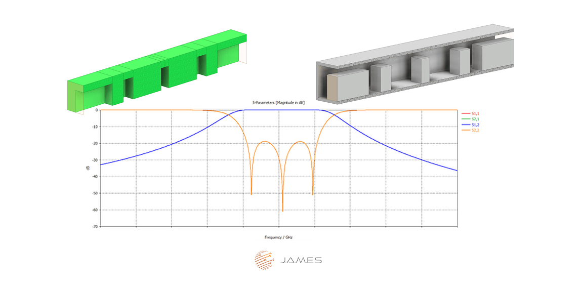
In this article we will discribe the exercise to reach out existing benefits by using the AMEway to realize high frequency waveguide filters.
With respect of
- very good RF-performance
- lightweight design
- reduction of manual assembling and tuning (save screws)
- testing of long term stability
Traditionally RF Waveguide filters have to work with
- increasing effords in mounting to reach out RF tightness
- many of screws
- manually tuning effords
for highest level of RF filter performance (e.g. high RF blocking attenuation; sharp separation of pass and stoppband etc.)
High frequency RF-Filters for product usecase in e.g.
- Avionics
- Defence & Space
- Automotive
- etc.
are on our tech roadmap to increase performance in the additive way.
If we can reach out good performing filter elements in a more lightweight element the
system benefit is increasing as well. So a satellite equipment for space communication will be more lightweight or a
plane can even fly longer.
The J.A.M.E.S Design activities will be supported by our partners to give innovative drive and to keep always product requirements and needs in focus with an industry partner established in this business area.
Acknowledgements:
We highly appreciate the support of Jonas Weindl and Alexander Paulus from TU-München, Chair of High-Frequency Engineering
Realisation Checkpoints
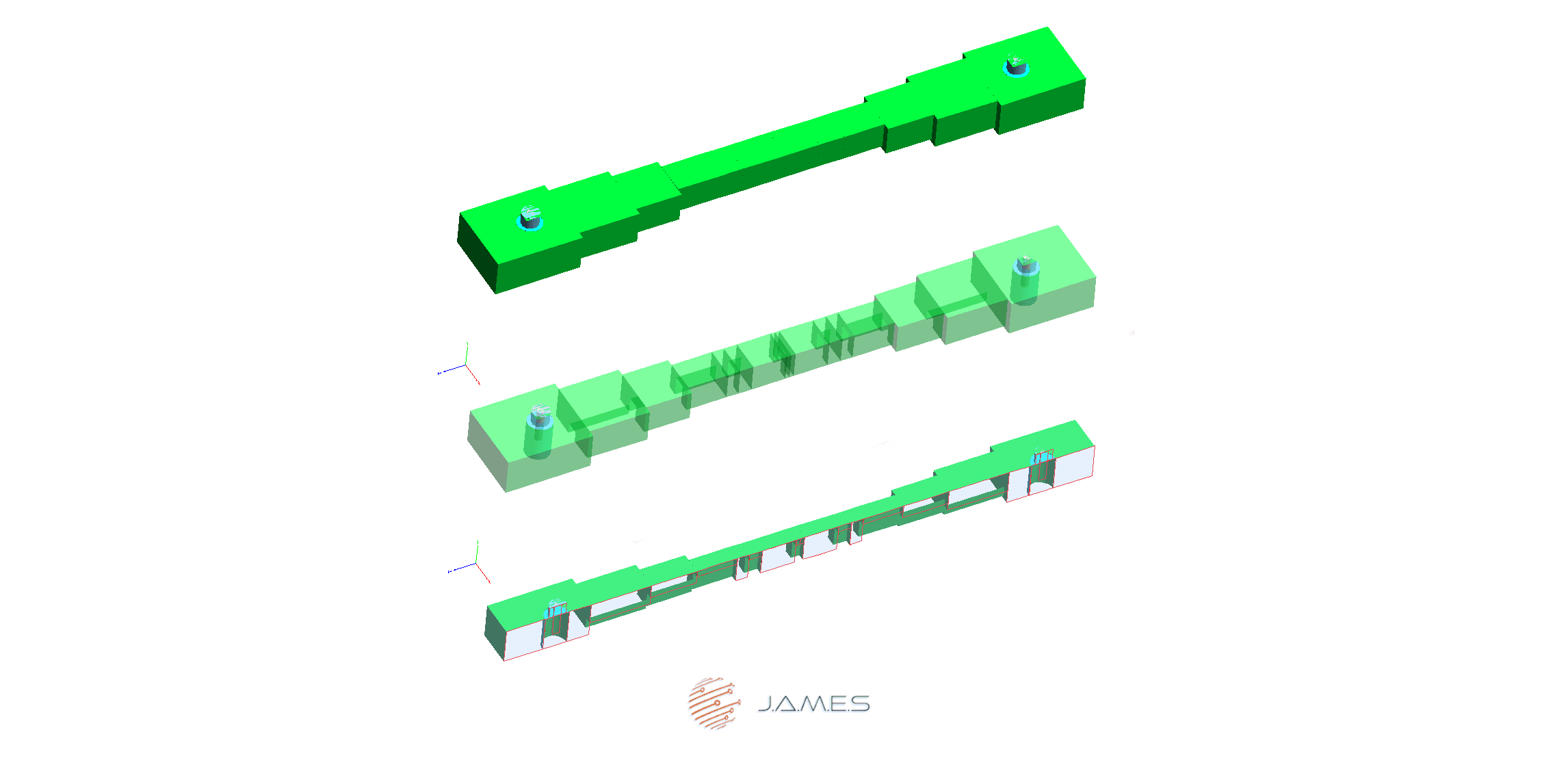
In order to acchieve very good electronic results, we have to check the performance of the
-
in form realization of the structural body (could be AM, as well)
- sharp edges
- AM with support material
- in body accuracy
- parallel walls etc.
- ...
-
for electronics and RF reasons there is an essential need of a conductive surface, at least
- complete AM conductive metal structure
- ? check for sufrace oxidation
- ? check selected conductive material
- border effects for precious metal transistions
- corrosion
- demodulation effects
- ? check for surface oxidation
- ? check for conductive surface thickness needed
- combination of a structural body with a post-metallication process
- ? check for restrictions in the metallization process
- e.g. for in body metallization - how to get the metalizing fluids in and out
- maximum metallization thickness which is possible
- edge accuracy after metallization (essential for RF-perormance)
- basic metallisation stability (to be able to implement a connector by screws etc.)
- ...
- ? check for restrictions in the metallization process
- complete AM conductive metal structure
-
With respect to the AM-/AME-printing, or post metallication process
- the operational requirements have to be taken into account
- weight
- degree of miniaturization
- mech. stability needed
- electronics performance (e.g. RF-filter behaviour) with own electrical requirements !
- environmental loads
- e.g. salt / sand / dust / humidity / temperature range (lots of more...)
- e.g. delamination stability and so on
- e.g. salt / sand / dust / humidity / temperature range (lots of more...)
- chemical robustness (e.g. for airborne equipment)
- you have to be careful whith this requirements!
- electonic applications in e.g. a UAV don't really see cerosine or killfrost impacts
- the operational requirements have to be taken into account
The decision for usage will be based on the performance and systems benefit!
Is the RF performance so good by reaching out a more lightweight system element it represents a perfect tuning components to make a bigger system more lightweight. (Systems engineers- & project leaders- & quality/safety engineers decision....and some courage)


