How AME Is Pushing Miniaturisation Boundaries

Smaller, lighter, more efficient. The drive for these kinds of devices is relentless, regardless of industry. In response, innovators, designers, and engineers everywhere are pushing the boundaries. Many are using miniaturisation to develop additively manufactured electronics (AME) with the potential to change how we interact with technology. Unlike traditional methods that bolt components onto circuit boards, AME integrates everything into the structure of the device.
Let's explore how this revolutionary approach is reshaping our future.
What Is Miniaturisation?
Miniaturisation makes things smaller, as the name suggests. It does this without compromising the object's functionality—it serves the same purpose but uses less space to do so. We can think of a typical smartphone as a good example. It's a phone, but it's also a camera and GPS. It tracks our steps and can even control devices throughout our home. It does all this and more while fitting into the palm of your hand.
Miniaturisation enables sleek and space-saving designs, but that's not its only utility. The size aspect of miniaturised electronics paves the way for all new possibilities. In aerospace, for example, every single gram counts. Lighter components make rockets more efficient and satellites more compact, leading to lower-cost space exploration. In healthcare, miniaturised implants require less invasive procedures. They can also open doors to more personalised, patient-focused treatments.
How AME Enables Miniaturisation
Traditionally manufactured electronics use a circuit board to hold all the various parts together. AME takes an entirely different approach. Everything is built from the ground up, one layer at a time. The components are not stuck onto a board—they become a part of the structure itself. This eliminates extra bulk and weight and reduces material usage.
AME is a technical and practical improvement, one that gives engineers the freedom to design in ways that simply were not possible before. They can forget the old rules of separate parts and cumbersome assemblies. Instead, they can design integrated systems that perform as one and take up significantly less space.
AME and Miniaturisation in Practice
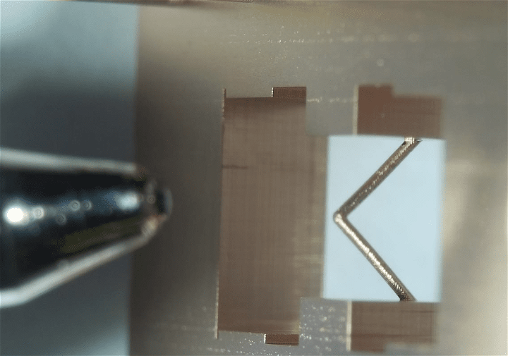
What might this all look like in practice? Traces, coils, and capacitors can be integrated directly into dielectric substrates. Let's investigate further.
Traces
Traces are the tiny conductive pathways that carry electrical signals through a device. Instead of using wires or bulky connections, AME prints these directly into the substrate. The result? Fewer failure points and better performance.
Coils
Coils are typically used for inductance and wireless power transfer and generally demand extra space to function. But, with AME, they are printed within the device's structure. This enables smaller, smarter designs for things like wireless charging or radio frequency applications.
Capacitors
Capacitors store and regulate electrical energy. Embedding them into substrates not only saves space but also reduces energy loss.
Looking to the Future
Looking ahead, miniaturisation and AME technologies could lead to a world where electronics are so small that they become almost invisible. They are embedded in our clothing or even our bodies, working behind the scenes to improve our quality of life.
It's an exciting vision that's about so much more than the devices themselves. It's also about greener manufacturing that uses fewer materials and generates less waste. Smaller components also mean lower transportation emissions.
Related Articles

MTC Honoured With Silver Award From Ministry Of Defence

Driving Innovation In 3D Printed Electronics: An Interview With Hanno Platz Of FED Working Group


