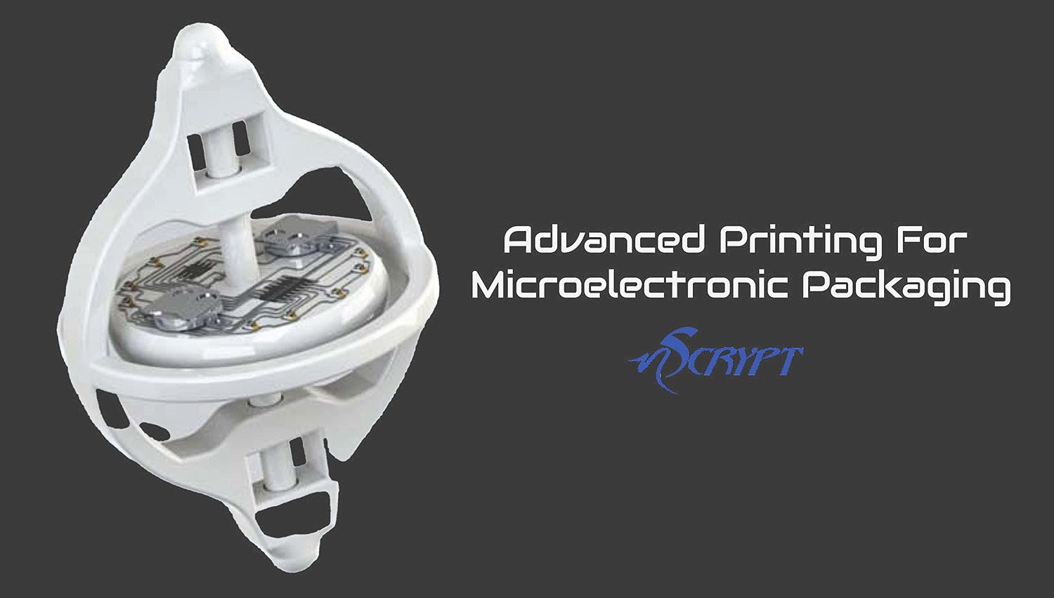
Advanced Printing For Microelectronic Packaging

This research paper "Advanced Printing for Microelectronic Packaging" was written by Kenneth H. Church, Xudong Chen, Joshua M. Goldfarb, Casey W. Perkowski, and Samuel LeBlanc from nScrypt, Inc.
Overview
The paper investigates advanced micro-dispensing technologies for 3D printing applications related to semiconductor packaging. Emphasis is placed on repeatable dispense volumes as well as the ability to use solders, epoxies, conductive adhesives, and ceramic-filled polymers. These materials are indispensable for building 3D structures and circuits in microelectronics.
nScrypt's micro-dispensing technology, powered by the SmartPump™, is capable of precisely metering small volumes, allowing for the creation of sub-50 micron features for conformal electronic circuits. This technology allows for the direct fabrication of complex, three-dimensional electronic components and circuits, eliminating the need for traditional soldering.
In an application-specific paper on the subject (Electronic Packaging and Materials), numerous other uses of micro-dispensing are addressed as well, such as printing tinier solder dots and adhesive spots with sub-nanoliter volumes. This approach showcases the future of printed electronics and also holds promise for monolithic electronic packaging - integrating circuits into structures.
Key Takeaways
Micro-Dispensing Technology:
When it comes to creating tiny, delicate electronic components, an enabling factor is precise control over the dispensed material volume. The SmartPump™ technology from nScrypt features a unique pen tip geometry and an X-Y position valve near the head, offering tremendous control, achieving dispensing of very small volumes (single-digit nanoliters or even smaller).
3D Printing in Electronics:
This will incorporate the employment of CAD/CAM (Computer-Aided Design and Manufacturing) methods to print around 3-D space, thereby making complex electronic circuits. Enables printing of different materials, including conductive adhesives and ceramic-filled polymers that are needed in modern microelectronic packaging.
Monolithic Electronic Packaging:
Electronics packaging trends in the future, where circuits become part of structures and eliminate traditional solder. Promises more compact, rugged electronic devices by increasing functionality per unit volume through advanced 3-D design techniques.
Applications and Benefits:
- Faster prototyping
- Easier electronic circuit production
- Increased functionality with less precision dependency
- Enables 3D structural and functional circuit printing without conventional assembly methods, offering enhanced design flexibility and streamlined manufacturing
Material and Process Control: Explains the necessity to control both dispensing height, flow rate of materials, and their properties (viscosity; thixotropy) in order to achieve uniform printing results. Hence, with respect to FD processes for ideal micro-dispensing outcomes, smooth surfaces finished are essential to ensure uniform material deposition.
Table of Contents
- Abstract
- Introduction
- Micro-Dispensing:
- Methods for Micro-Dispensing Small Solder Dots
- Micro-Dispensing Fine Adhesive Features
- 3D Printed Structures Using Micro-Dispensing and Fused Deposition
- Conclusion
- References
Conclusion
The use of micro-dispensing technology is a major advancement for electronic packaging, offering precise control over small volumes and enabling the creatiion of intricate, highly functional electronic devices. The SmartPump™ has the potential to revolutionize the industry by supporting smaller features, integrating circuits within 3D structures, and replacing traditional solder methods. This technology enables fast prototyping, less complex manufacturing, and contributes to more compact, efficient electronic devices, positioning it as an important contributor to the future of advanced packaging in electronics.
See the 3D Manufacturing Process of a Printed Cylindrical Circuit by nScrypt
This fully 3D-printed, cylindrical printed circuit (PCC) was manufactured entirely on an nScrypt 3Dn-500 with a 100mm rotary stage attachment.
The device is made from PC-ABS plastic with integrated silver traces. Key features include:
- An embedded Bluetooth microcontroller
- A printed antenna
- An array of fully embedded sensors
These sensors support components such as acoustic, light, and motion sensing.
Related Articles

FED White Paper Edition 2024 - AME Classification Overview

Functionalization Of Additively Manufactured Ceramic Components Via Thick-film Technologies

Revolutionizing Display Manufacturing: The Impact Of XTPL’s Ultra-precise Dispensing Technology


