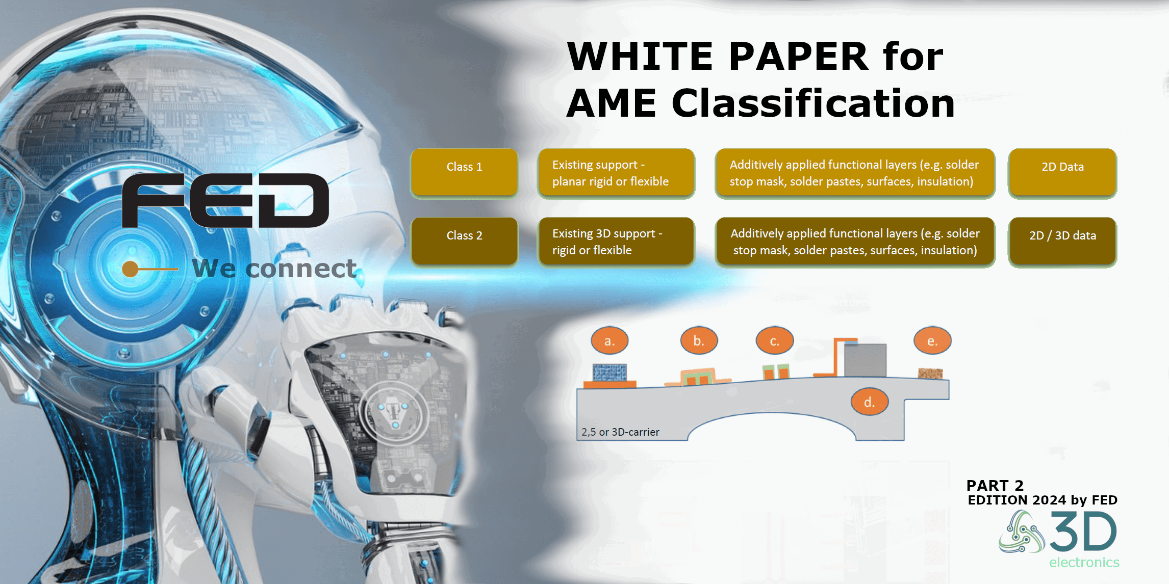
FED White Paper Edition 2024 - PART 2 - AME Class 1 And Class 2

Part 2,
Explaining AME Class 1 and Class 2
of the new edition White Paper
Classification of additive manufacturing and 3D-printing processes for electronics
Table of Contents
Classification of Products Using Additive Manufacturing (AM) Methods
As already described in PART 1, the use of the various AM methods will continue to increase as different advantages become more apparent. At the same time existing AM methods are constantly being improved and new, methods are being developed. Due to the large number of processes and applications it makes sense to classify the methods from a general perspective of product manufacture. The “FED 3D Electronics Working Group” has drawn up a classification in a two-year project.
The basic idea is, that the different classes build on each other. Many different technologies and methods can be used for application of materials on flat surfaces. Many of these technologies based on classic printing technologies, in which the surface is touched (contact). For uneven surfaces or three-dimensional shapes contactless printing processes has a high potential, other methods are used. These processes are associated with "3D Printing" and "Additive Manufacturing" (AM).
With each class the requirements for complexity and handling as well as printing technology and precision increase.
The classification is intended to provide a classification model for the various facets of partially or fully Additively Manufactured 3D electronics. In the model described here this is done on a simplified basis and divided into five classes, to illustrate the basic information for differentiating between the classes. Further details follow on the next pages of the document.
FED classification for Additive Manufacturing used Electronic manufacturing
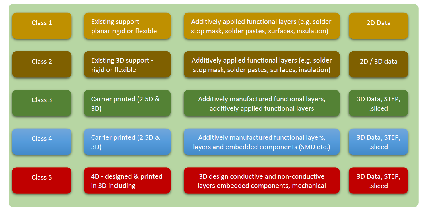
The “FED 3D Electronics Working Group” defines five classes of Additively Manufactured Electronics with increasing complexity that build on each other
Class 1 – Basic Class, 2D-Substrate (carrier) and Printing
The “Basic class 1" defines the application of one or more conductive, semi-conductive or non-conductive functional layers on an existing planar substrate (2D). The printed material can be rigid, flexible or stretchable. The substrate can consist of almost any material: printed circuit board substrate, ceramic, metal, plastic, textile, paper, cardboard and others.
The typical products for this class are referred to as "printed electronics".
Material Application
The additively applied functional layers can be created in a variety of ways. In the simplest case and as known from classic printing technology, by gravure printing or screen printing. These two technologies are often used for so-called "printed electronics". Additive application techniques also include numerous other processes such as:
From the perspective of electronics production or pcb manufacturing an easy example of an insulating layer is 3D-inkjet-applied solder resist. Examples of conductive structures include the printing of electrical functions or components such as antennas, sensors, filters or contact points.
If the insulation material is applied in one or more steps together with a conductive (semi-conductive) material, three-dimensional structures can be produced on the available carrier substrate, for example. The multi-layered conductive layers can be separated by local and partially applied insulation layers, among other things.
Another example is the application of specific surface materials, Application of functional sensor layers, e.g made of nanomaterials with gold or other metals. Connecting materials can also be applied additively, such as sintered material or heat-conducting layers.
Additively Manufactured Electronics Class1 - Definition by FED
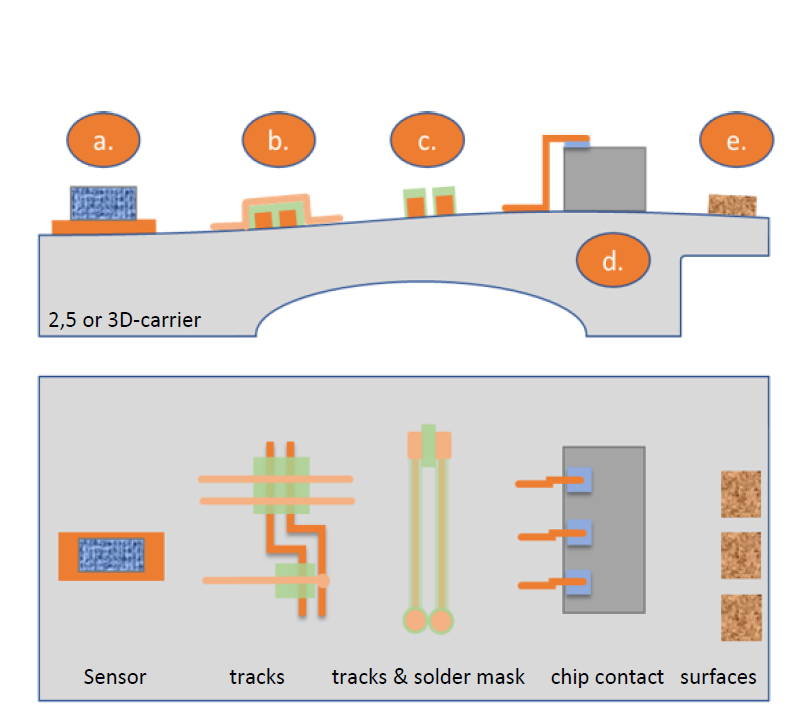
a) The base or carrier material could be a textile, printed circuit board with or without conductor tracks, foil, ceramic or plastic part or paper.
b) The substrate can be rigid, flexible or stretchable, but it is in production process flat.
c) Additive layers can be produced by screen printing, paste or ink printing or other processes in various heights (thin structures).
d) Optionally, conductive materials or layers with which, for example, additive conductor structures or insulating layers are produced, such as the 3D solder resist or other insulations.
e) Another variant is the application of, e.g.: resistance material, for electrical functions and other components or functions, such as resistors, coils, antennas, sensors.
f) The application of special surfaces, such as gold coatings or nanomaterials for contact points, or additional bonding materials such as solder or sintering pastes and adhesives.
AME Class 1 - EXAMPLES
Examples of materials that are applied (printed) on different types of substrates
Class 2 - Multidimensional Carrier (substrate) + Printing
The “Class 2" defines the application of one or more conductive, semi-conductive or non-conductive functional layers on an existing multidimensional substrate, which can be rigid, flexible or stretchable. As described in "basic class 1" the additive layers can be applied using a wide variety of processes and technologies. Multilayer conductor layers can also be separated by partially applied insulating layers.
As with multidimensional moulded carrier, placed components or functions can be directly printed with material in the event of a height difference and thus connected to each other electrically, thermally or for other purposes (e.g.: light guides). The typical products for this class are referred to as "3D MID".
Another option i.e. in “In mould Technology” (IME) is to reshape the printed layers into a new 3D contour in a further and additional process step.
Additively Manufactured Electronics Class2 - Definition by FED
a) Optionally, sensor or antenna struc-tures can be applied (e.g.: using dif-ferent angles).
b) Multilayer conductor layers can be separated by partially applied
insulation layers.
c) Partially applied solder resist or pro-tective coating.
d) Components with height differences can be connected directly with con-ductor tracks be contacted.
e) Special surfaces: Gold, nanoparticles or additional composite materials such as solder or sinter paste.
Go Back to AME Classification Overview
the FED working group for 3D electronics is
Introducing the 5 Classes/Types of process 3D printed electronics
Related Articles

J.A.M.E.S Overview - New Materials, Processes And Applications For 3D-printed Electronics "AME"

Driving Innovation In 3D Printed Electronics: An Interview With Hanno Platz Of FED Working Group


