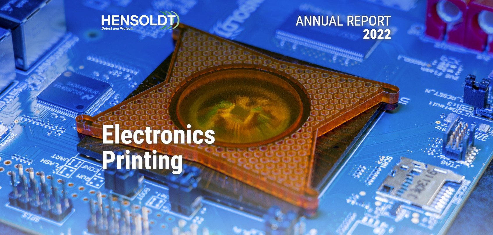
Electronics Printing

The printing of three-dimensional objects is being used commercially by more and more industries.
How HENSOLDT Is Bringing 3D Printing to the Electronics Sector
HENSOLDT is going one step further and is driving forward the 3D printing of electronics. This creates completely new design possibilities for electronic components. Development cycles are becoming shorter, and costs are falling. The potential applications are extremely diverse across all industries.
HENSOLDT is creating electronics in a new way – and is also breaking new ground entrepreneurially: Together with Nano Dimension, an Israeli specialist in 3D printing, HENSOLDT founded the joint venture J.A.M.E.S in 2021 and created a platform for agile, collaborative research. J.A.M.E.S stands for “Jetted Additively Manufactured Electronic Sources” and refers to one of the great future technologies of 3D printing: printed electronics, also called AME (Additively Manufactured Electronics).
With the help of special inks, it is possible to design electronic components directly via the printer and bring them into a three-dimensional form. In this way, particularly sophisticated electronic components can be manufactured quickly and easily. If at all, this would only be possible with conventional manufacturing methods at great expense and with high susceptibility to errors.
For several years now, HENSOLDT has been investing in basic research into this new technology and, together with Nano Dimension, is driving forward the “technology readiness level” of printed high-performance electronic structures. J.A.M.E.S combines the strengths of both participating companies in this field and enables an easy entry into this innovative technology.
A Worldwide J.A.M.E.S Community – Countless Insights
To connect the diverse development approaches and to drive progress in partnership, J.A.M.E.S has launched the first comprehensive online community for 3D printed electronics. On a cloud-based platform, experts from all parts of the world come together to further develop the processes for additively manufactured electronics – from students and scientists to start-ups and experienced engineers. Easily accessible, the J.A.M.E.S library connects the accumulated knowledge with concrete applications. Independent research – enabled by HENSOLDT – leads to new insights and concrete results that can later be applied to the manufacturing of electronics for military and civilian applications.
From 3D to 3D Electronics Printing
In the three-dimensional printing of mechanical objects – known as “Additive Manufacturing” (AM) – layers of material are applied step by step. The process has been around for more than ten years and is now used in numerous production facilities. Accordingly, a large number of proven materials and processes are available. Also, HENSOLDT is using the numerous advantages of 3D printing for more and more products. For example, in the case of the fully digitalized “Kalaetron Attack” interference system, metallic 3D printing allows for particularly compact dimensions for the HENSOLDT solution, thus facilitating integration into aircraft.
The still young discipline of three-dimensional printing of electronics – “Additively Manufactured Electronics” (AME) – goes a decisive step further: It produces the electronic components of circuits such as conductive connections, coils, capacitors, or antennas. It also produces the associated heat sinks, housings, and other structures for an application. In other words, the entirety of components that actively contribute to electrical functionality and those structures that enable and support this functionality are printed.
As the first process already available, Nano Dimension’s DragonFly IV printer system can print AMEs based on two different inks: a photopolymer ink cured by ultraviolet (UV) light can produce low- or non-conductive structures – for example, insulating materials and insulation, but also components of antennas. An infrared-cured silver nanoparticle ink is used to create electrically conductive structures.
Another process already available enables very small conductive lines to be applied to existing surfaces. With additional technologies such as the ceramic-based processes of the Fraunhofer Institute for Ceramic Technologies and Systems, ceramic materials can be electrified – often central for applications under extremely high temperatures or other harsh environmental conditions.
AME – the Electronics of the Future
AME is considered one of the great technologies of the future. 3D printing of complete electronic components offers greater design freedom and faster development times and enables significantly more compact and cost-effective devices. The printed electronic components can be tested, adapted, and verified before production begins. This pays off, especially for small series and individualized single parts. In addition, completely new applications become possible. Initial concepts illustrate virtually unlimited possibilities.
With AME, HENSOLDT not only wants to accelerate the development cycles of its solutions further. The targeted production of electronic spare parts can also be significantly simplified and thus customer needs can be satisfied faster and more cost-effectively.
Related Articles


