Introduction To CerAMfacturing At Fraunhofer IKTS
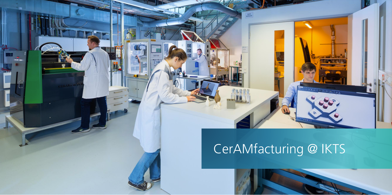
This article provides you a full insider perspective with expertise and competence behind 3D ceramic technology
by Uwe Scheithauer and Lars Rebenklau, Fraunhofer IKTS (Fraunhofer Institute for Ceramic Technologies and Systems IKTS)
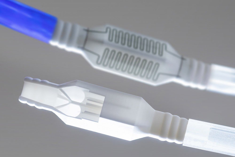
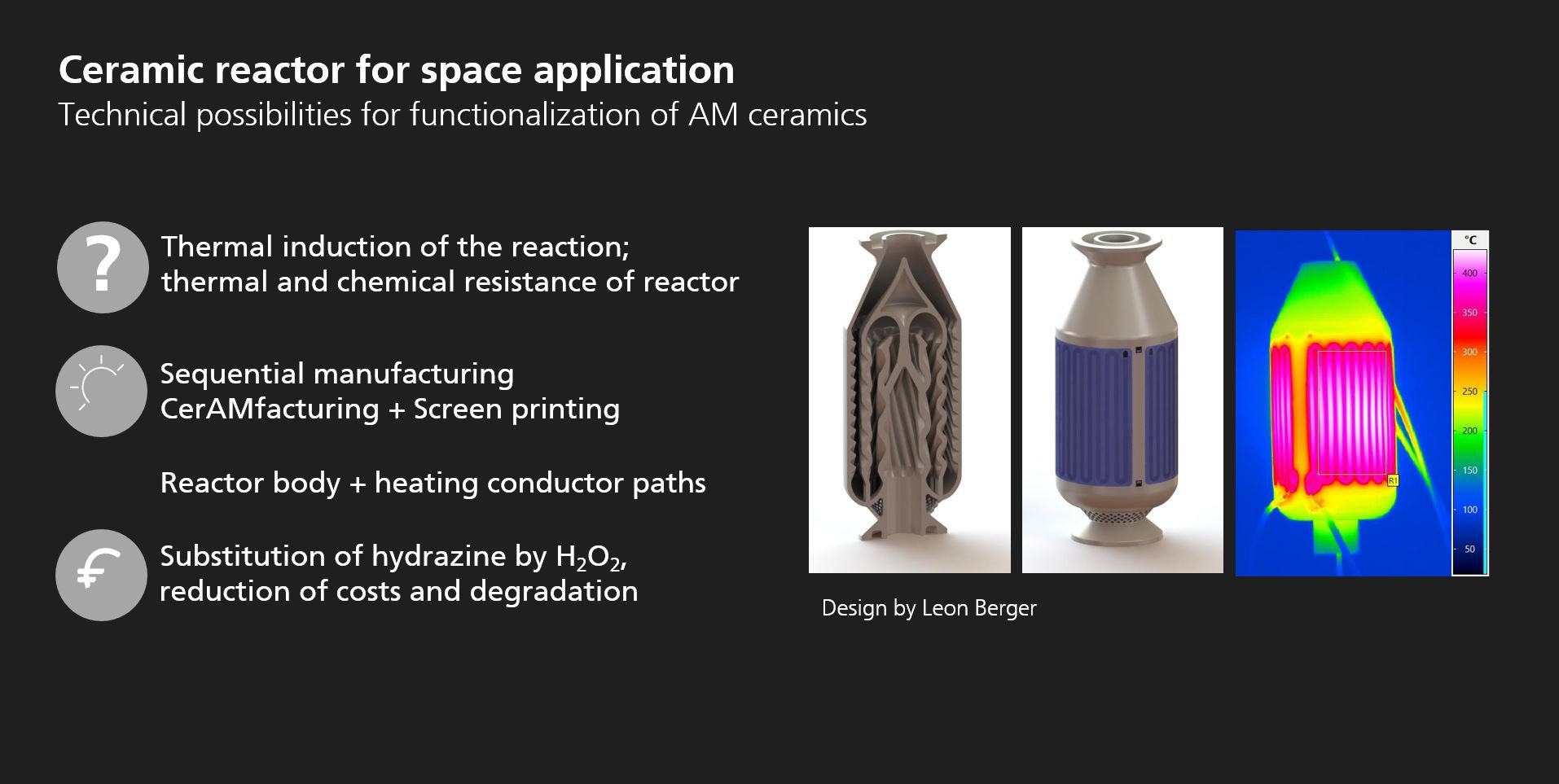
Functionalization of AM ceramic components via thick-film technologies
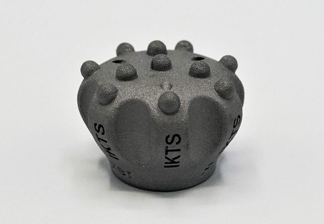
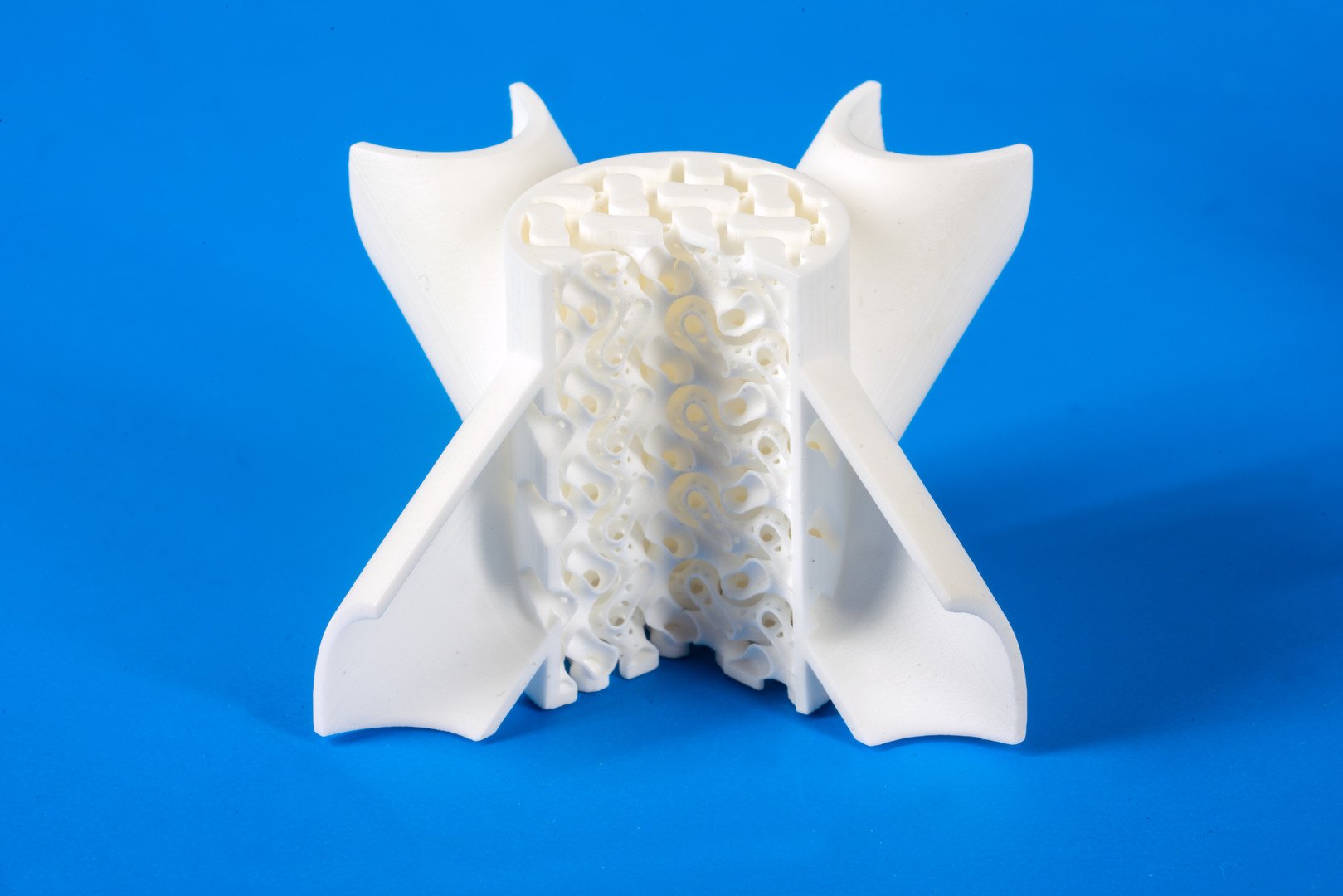
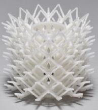
Advanced ceramics have combinations of properties that other classes of materials cannot achieve. They are characterized by very high thermal, chemical and mechanical resistance. By adapting additive manufacturing processes for ceramic materials (CerAM), ceramic components can be complexly shaped, further functionalized and miniaturized – as is common for other classes of materials.
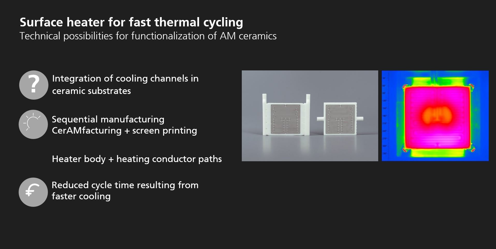
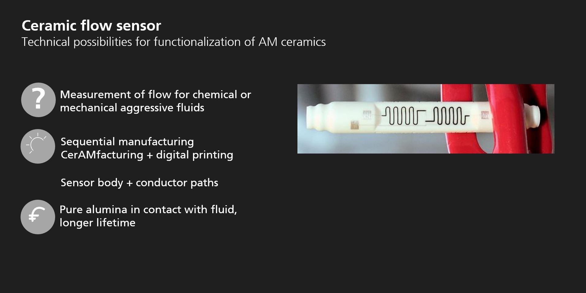
Functionalized components can be realized by combining ceramic additvie manufactuirng and thick-film technologies. In a first step, the ceramic basic component is manufactured, including sintering. In a second technological step, this ceramic component is functionalized. For Al2O3 as well as other ceramics, the thick-film technology established in electronics and microsystem technology is a good solution. This technology can be used to print and fuse electrical conductors, resistors, heating elements or sensors onto the ceramic substrates. The electrical connection contact is realized by proven methods of the packaging technology of electronics. The advantage of this approach is that the materials required for functionalization are available on an industrial scale.
Different AM technologies at IKTS
Fraunhofer IKTS offers complete AM solutions ranging from powder and suspension/feedstock development and production method selection to functionalization and quality control of novel parts and systems. The following methods are availabe:
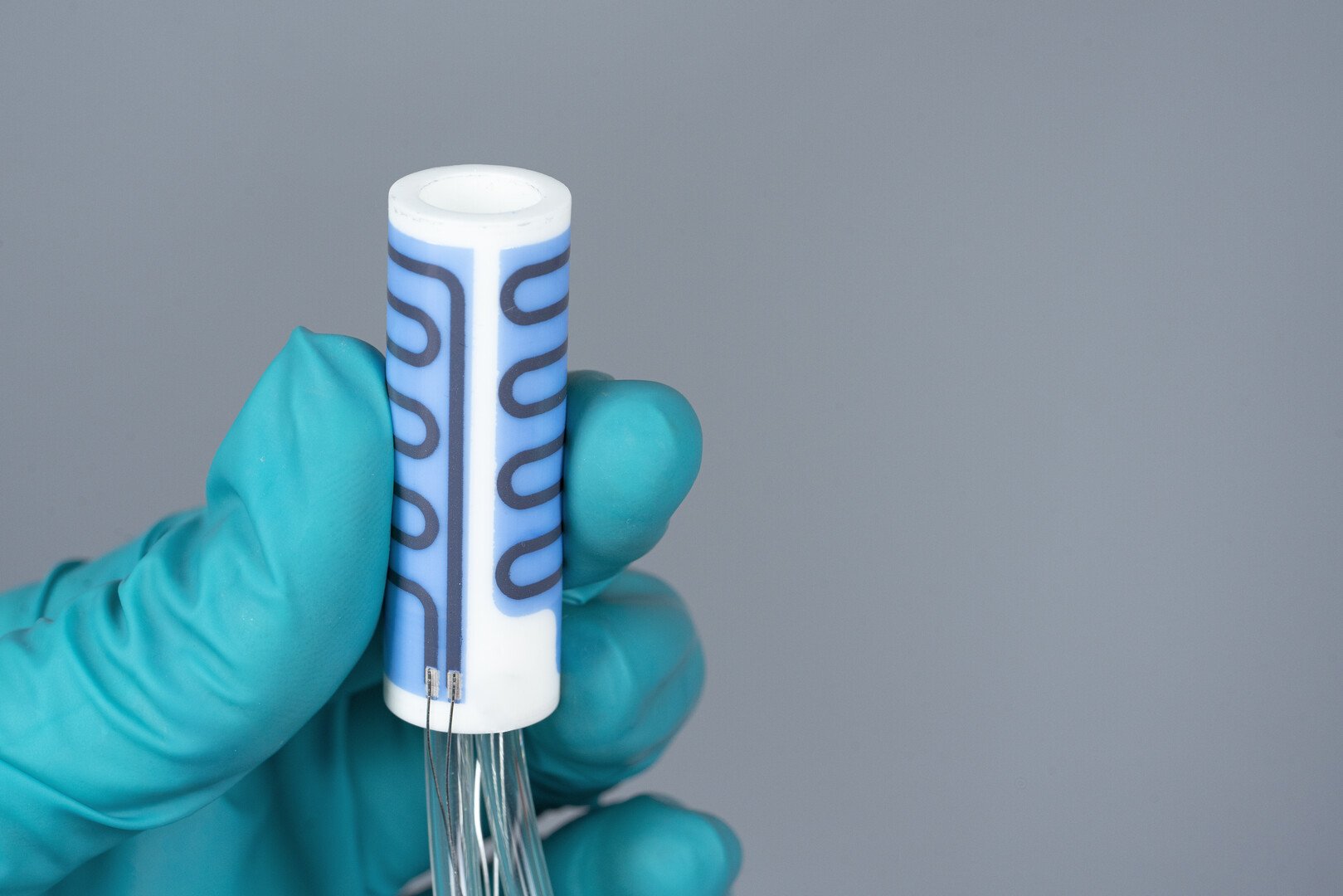
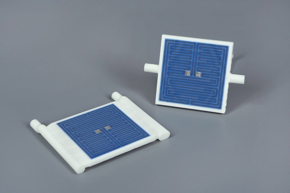
AM functionalization using thick-film technologies
Highly integrated functional components for electronics, analytics, sensors and process technology
Download the full white paper prepared by Fraunhofer IKTS
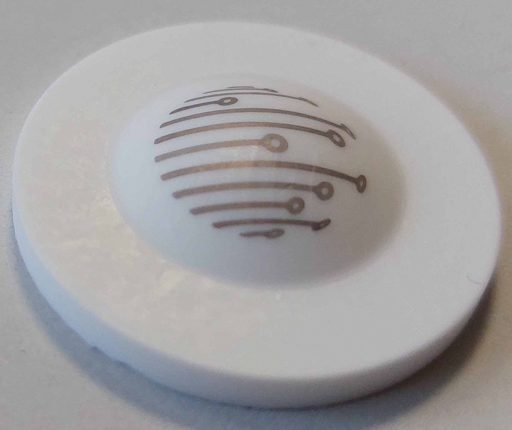
Read more about the J.A.M.E.S Coin NFC On AME in 3D Ceramics
For the first time the J.A.M.E.S Coin Design is transformed into a new material and process concept. The Fraunhofer IKTS at Dresden used their process knowledge in additive ceramics to realize the NFC tag application.
By utilizing ceramics and the additive process to integrate conductive structures into the J.A.M.E.S coin's formfactor, we can unlock a range of material and process advantages. This approach offers improved thermal stability and radiofrequency capabilities, opening doors for future applications.
Related Articles


FED White Paper Edition 2024 - AME Classification Overview

Additive Manufacturing Of Interposers With Curved Vias For Microelectronics Packaging

Design And Fabrication Of A Plastic-Free Antenna On A Sustainable Chitosan Substrate

