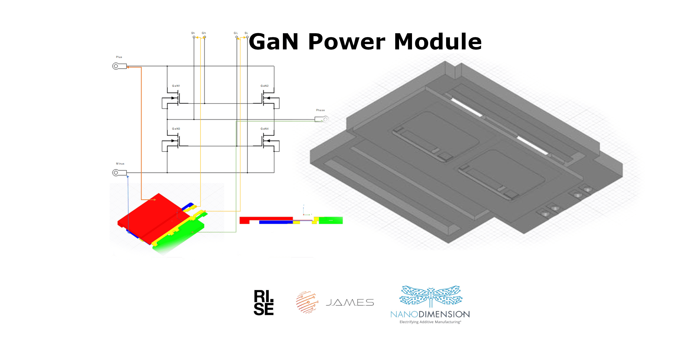
3D Printing Electronics For GaN Power Module Packaging At RI.SE

RISE GaN Power Module project
Summary Report
This article presents a collaborative project between RI.SE and Nano Dimension. The aim of the project is to use a GaN-based transistor to create a half-bridge device.
The first phase of the project involved printing a package for a GaN-based DIE component. The follow-up project will create a half-bridge module utilizing this package.
The device’s mechanical characteristics are approximately 64% smaller than the smallest similar functional devices existing in the market and will achieve the highest power density for this type of device.
Furthermore, this is the first attempt to use 3D AME technology to reduce size, decrease manufacturing time, and improve power density in this type of circuit.
Special thanks to Author: Ido Karpankop and Co-author: Hodaya Hovesh and Klas Brinkfeldt (Research Institutes of Sweden (RI.SE))
AME Background
Additively manufactured electronics is an emerging approach that takes printed electronics into the third dimension. Printing both structural material and conductive traces offers benefits that include extensive design freedom, rapid development iterations, and more compact devices.
The following design includes four GaN transistors embedded in a 3D printed module (half-bridge GaN power module).
The conductive layer of the module was printed with silver-based conductive ink and sintered using an IR lamp. The dielectric layer was printed using polymer-based ink and cured with a UV lamp.
The design is based on the GaNPx Package and transistor specification
- Manufacturer: Infineon (formerly GaN Systems)
- Component type: GS66516T
- Package: GaNPx
- Chip type: GS66516D2
Optimization and Test of Conductive Layer Design
Two optional conductive layer designs were tested: mesh and plain.
Conclusion and Outlook
This pioneering AME work, together with RI.SE and Nano Dimension, offers a great perspective into the field of power electronics.
The results show the high current performance and usable range of a custom-designed package (referred to as GaNPx package by Infineon, formerly GaN Systems Inc.) using the MultiJet-System DragonFly IV and the provided functional inks (CI conductive ink with silver nanoparticles and DI photopolymer).
J.A.M.E.S Remark:
It is worth mentioning that with 3D printing of electronics, the design variation perspectives offer incredible possibilities for use case optimization. Even materials that are supposedly thermally weak prove to be usable within limits. Increasing the AME process and the availability of specialized materials is crucial.
Special applications and requirements, such as power electronics, necessitate special materials that are processed additively. An excellent example of a material particularly suitable for extreme conditions is ceramic, which can be additively realized in unforeseen form factors using 3D printing. Through the additive processing of conductive and non-conductive materials, the robust base material proves to be optimal for applications in power electronics, though it still has its feasibility limits.
Empowering research investigations for 3D design tools will be relevant. Accept and understand how excellent material properties are exploited through various additive processes. There is no “one size fits all solution”! However, there are new smart solutions that make effective use of the various advantages of different processes and materials.
For high current and rugged use cases, J.A.M.E.S recommends:
Keep AMEfication Power in mind and contact J.A.M.E.S consultancy for support in making the right decision for Power Module Packaging.
Comments
Related Articles

Nano Dimension And Horizon Microtechnologies: Next-Level Innovations At European Microwave Week In Paris


