Explaining The CerAM Vat Photo Polymerization Based On JAMES Coin Design
Article by Eric Schwarzer-Fischer, Nadine Lorenz and Uwe Scheithauer, Fraunhofer IKTS (Fraunhofer Institute for Ceramic Technologies and Systems IKTS)
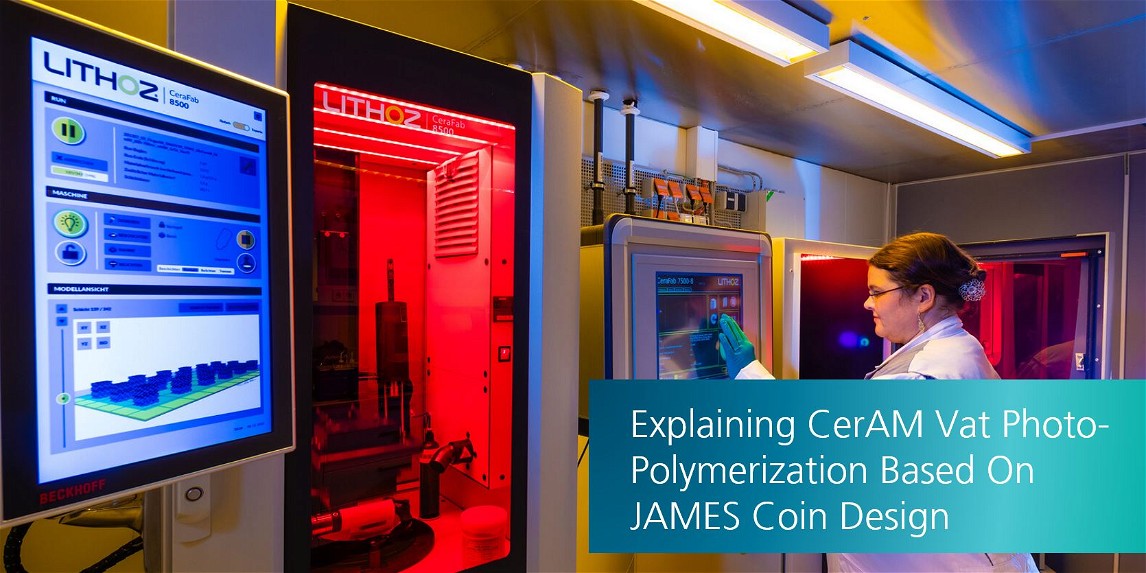
Explaining the CerAM Vat Photo Polymerization
Introduction to the Lithoz LCM technology
The Fraunhofer Gesellschaft IKTS is working with the CeraFab 7500/8500 systems (by Lithoz)

The Basics of Photo Polymerization
How is it possible to create a homogeneous 3D structure out of a ceramic powder ?

Introduction to the ceramic process chain
Based on the example of the JAMES Coin a flowchart gives an overview of all relevant and performance driving stations of the 3D ceramic process.

Example: Realization of the JAMES Coin in 3D ceramic
What are the process steps to create a ceramic JAMES Coin formfactor?


Read more about the J.A.M.E.S Coin NFC On AME in 3D Ceramics
For the first time the J.A.M.E.S Coin Design is transformed into a new material and process concept. The Fraunhofer IKTS at Dresden used their process knowledge in additive ceramics to realize the NFC tag application.
By utilizing ceramics and the additive process to integrate conductive structures into the J.A.M.E.S coin's formfactor, we can unlock a range of material and process advantages. This approach offers improved thermal stability and radiofrequency capabilities, opening doors for future applications.

Introduction To CerAMfacturing At Fraunhofer IKTS
have a full insider perspective with expertise and competence behind 3D ceramic technology
Related Articles

Simultaneous Manufacturing And Co-Sintering
To allow the integration of the functional materials also inside the component, which results in a higher degree of freedom concerning the design, simultaneous manufacturing is used.

Design And Fabrication Of A Plastic-Free Antenna On A Sustainable Chitosan Substrate
"Design and Fabrication of a Plastic-Free Antenna on a Sustainable Chitosan Substrate" by I. Marasco et al., 2023.
TactoTek And Essemtec: Printed Electronics (Case Study)
Printed electronics have gained significant acceptance in the electronics industry due to its versatile functionalities in various manufacturing processes.
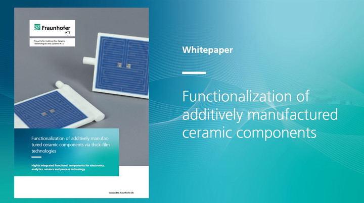
Functionalization Of Additively Manufactured Ceramic Components Via Thick-film Technologies
by Lars Rebenklau, Fraunhofer IKTS (Fraunhofer Institute for Ceramic Technologies and Systems IKTS) The whitepaper provides a simplified overview of the basics of thick-film technology and its ...

Flexible Quantum-Dot Light-Emitting Diodes Using Embedded Silver Mesh Transparent Electrodes Manufactured By An Ultraprecise Deposition Method
Flexible substrates with transparent conductive electrodes (TCEs) are essential components of organic-light-emitting diodes (OLEDs). However, Indium tin oxide (ITO), the prevailing transparent and ...

Durability Investigations Of 3D Printed Electronics Towards Aeronautic-inspired Environmental Loads
Together with AIRBUS Central Research and Technology J.A.M.E.S engineering established collaboration activities in field of 3D printed electronics with interest for aeronautic usecase. AME printed ...